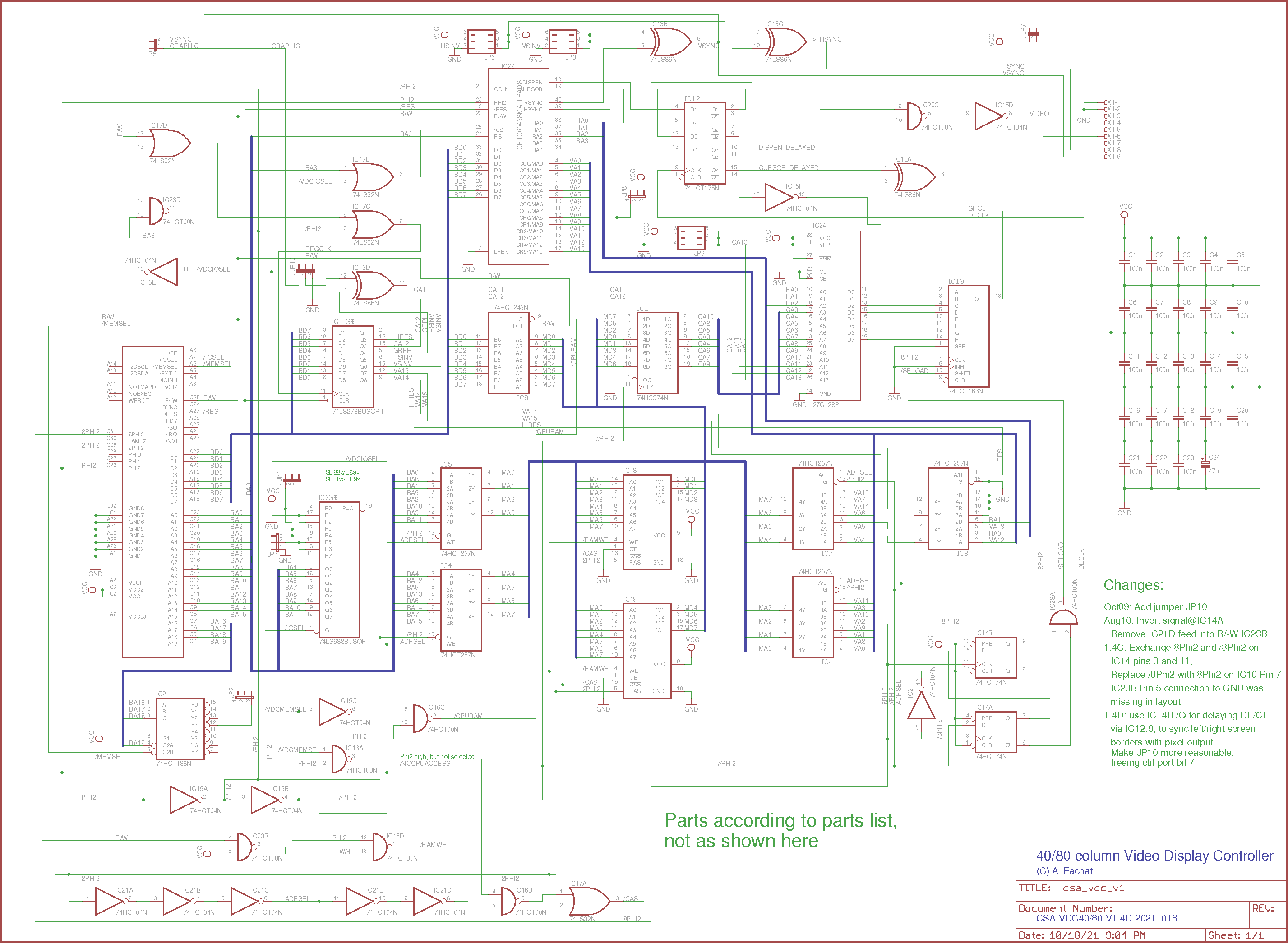
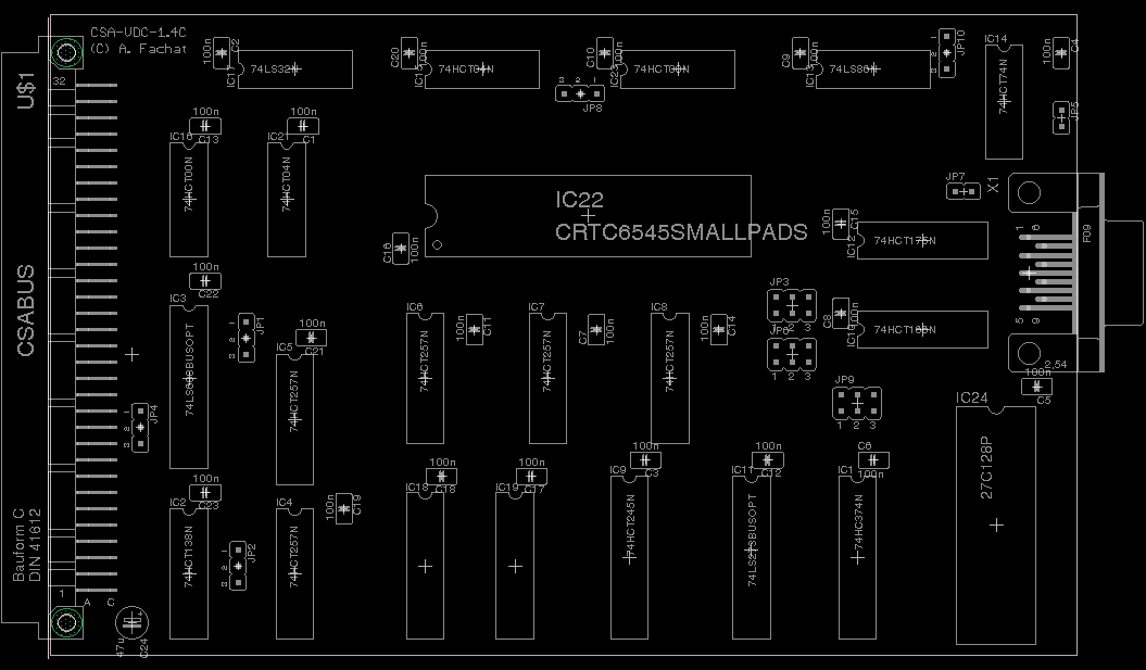
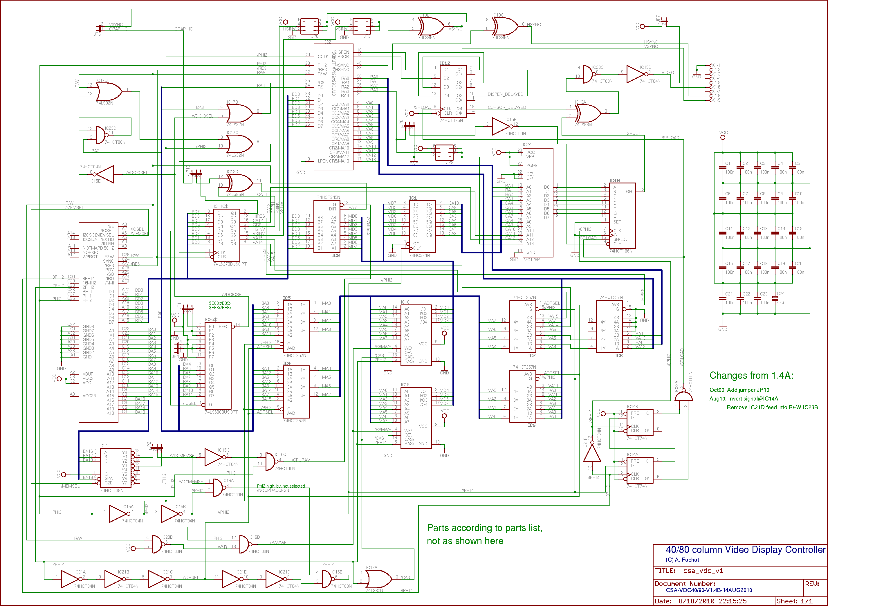
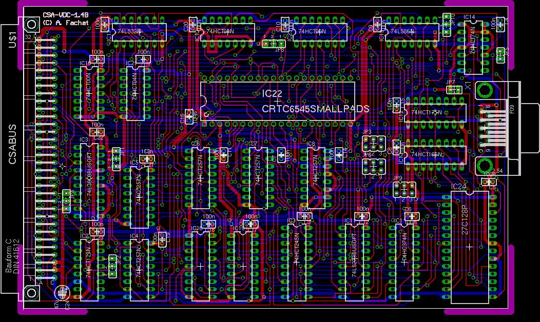
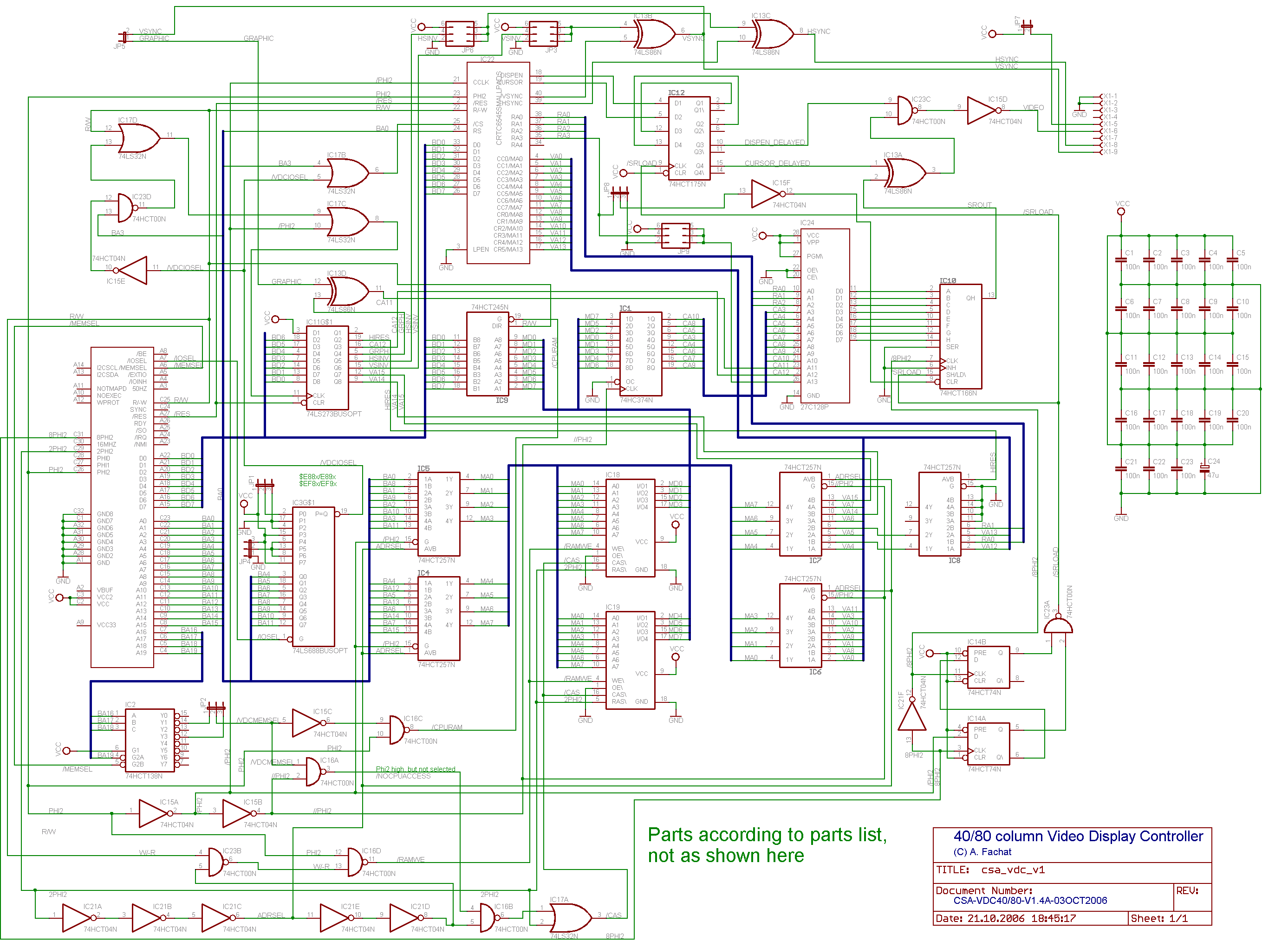
CS/A65 Video board
This board implements the a video board for the CS/A65 bus.
The board uses 64k dynamic RAM that is accessed in a
time-shared way, by the CPU at Phi2 high, and by the
video at Phi2 low. Due to this interlock the board can
display 40 columns a line at 1MHz system clock, and 80 columns
a line at 2MHz system clock.
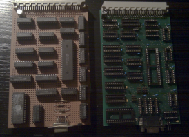
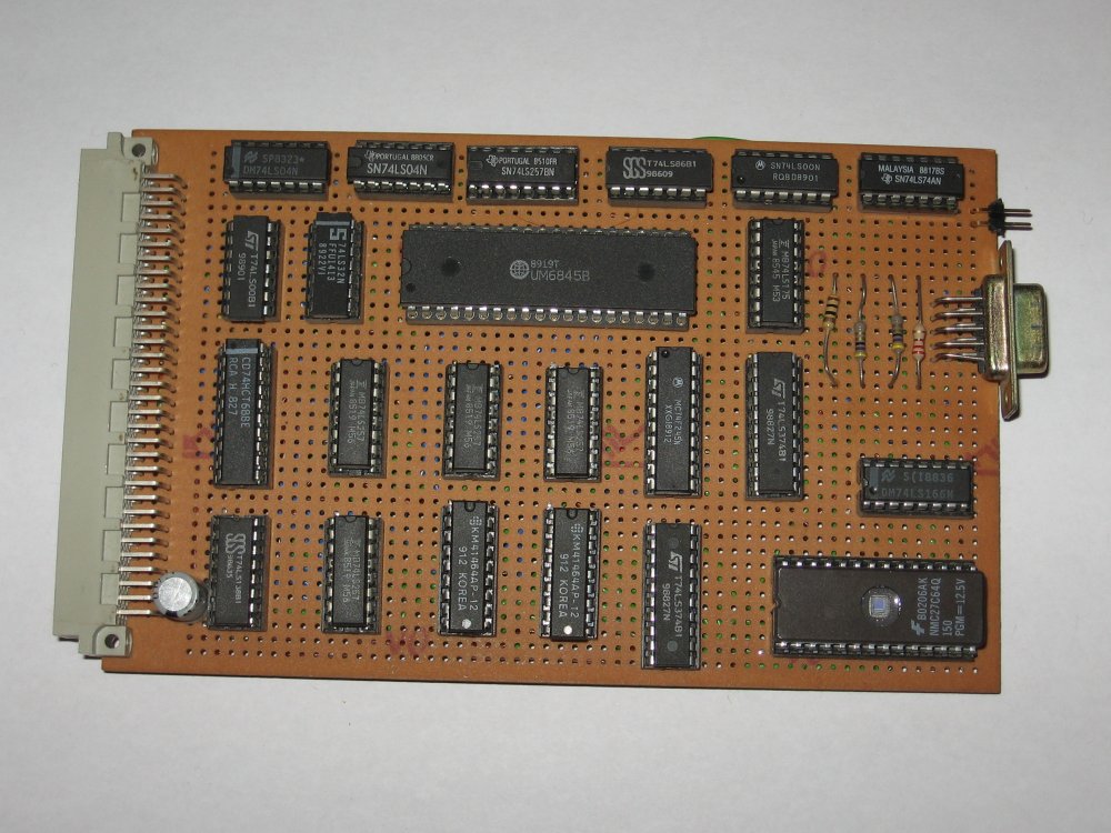
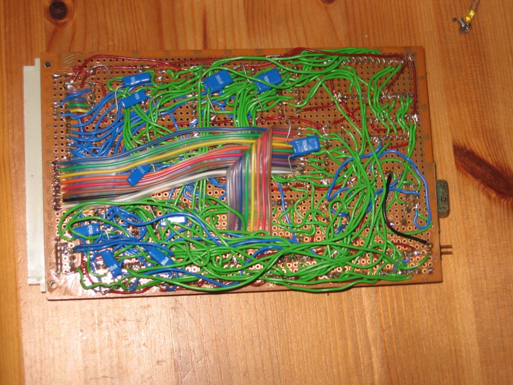
The old and the new version front ...
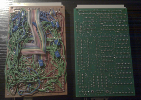
... and back side. What a difference!
Please note that to get a composite video signal, you need an extra circuit on the video connector.
You can find some on the composite video page

The old and the new version front ...
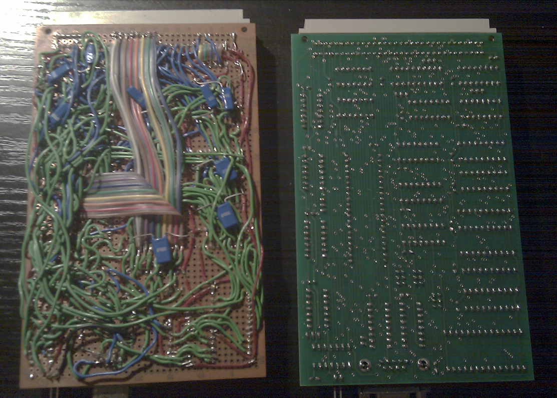
... and back side. What a difference!
- 2021-10-17 With a better screen you could see that display enable was about half a pixel off ... Updated to version 1.4D
- 2011-05-04 It's amazing how quickly you can find problems with a good scope. Updated to version 1.4C.
- 2010-12-20 Separated the composite video generation circuits into their own page.
- 2007-06-29 Added helper boards that convert the video signals to composite video.
- 2006-11-01 Added driver code.
Table of content
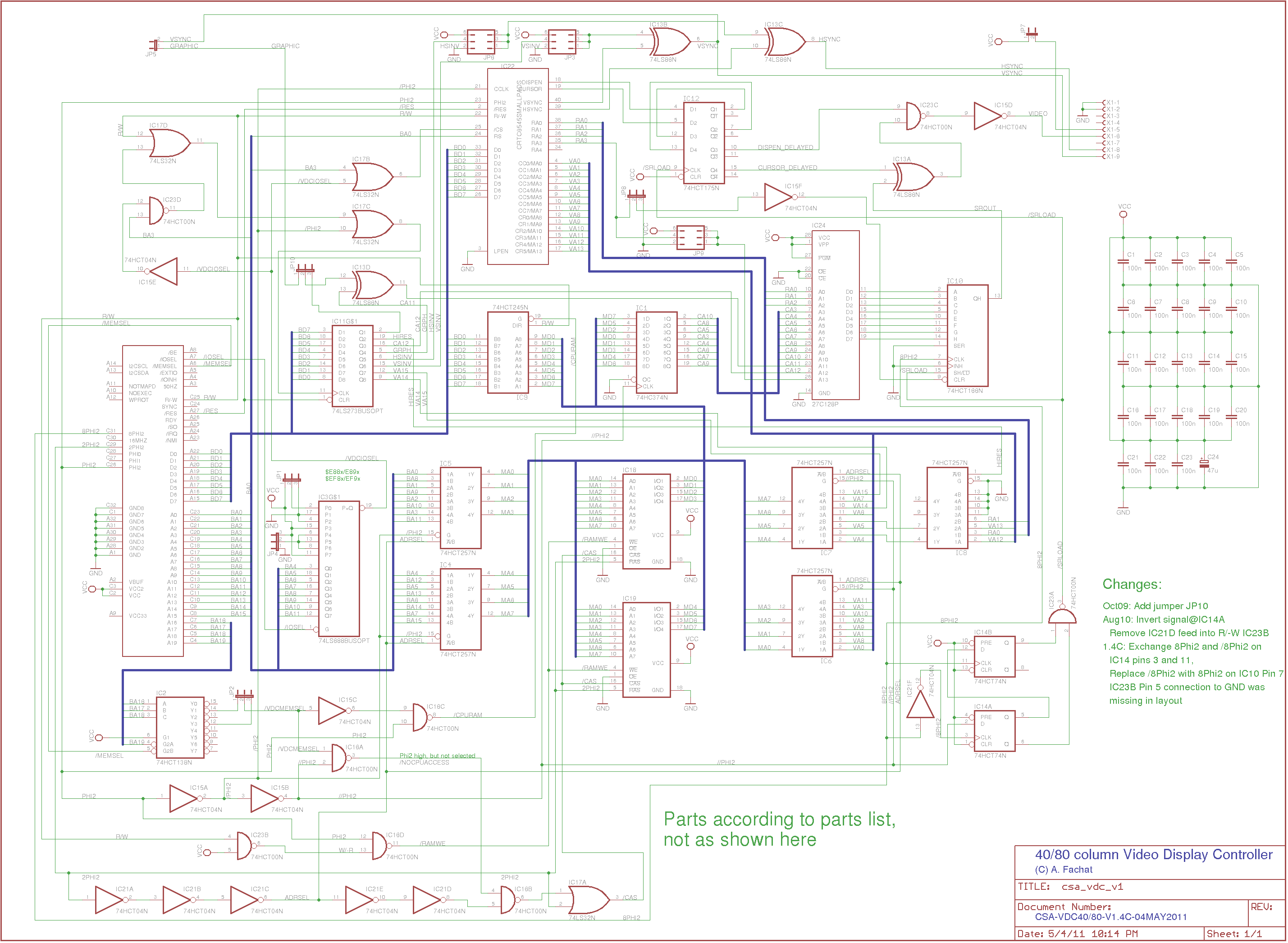
OS/A65 VDC hardware driver
This is the video-specific hardware part of the
CS/A65 console driver. It provides the following
methods:
inivid- initialize video hardwaresetact- set the CRTC display address to the current screencrsron- set the CRTC cursor to the correct address (the hardware cursor is actually flashing all the time)
freq variable.
| con_csa.a65(VDC driver excerpt) |
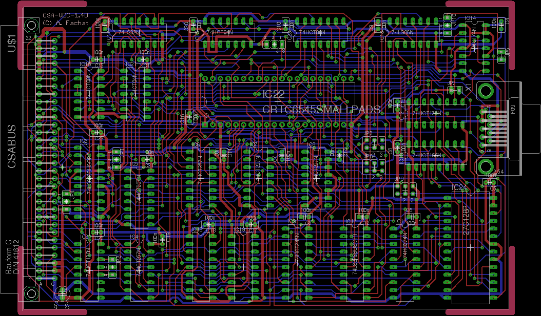
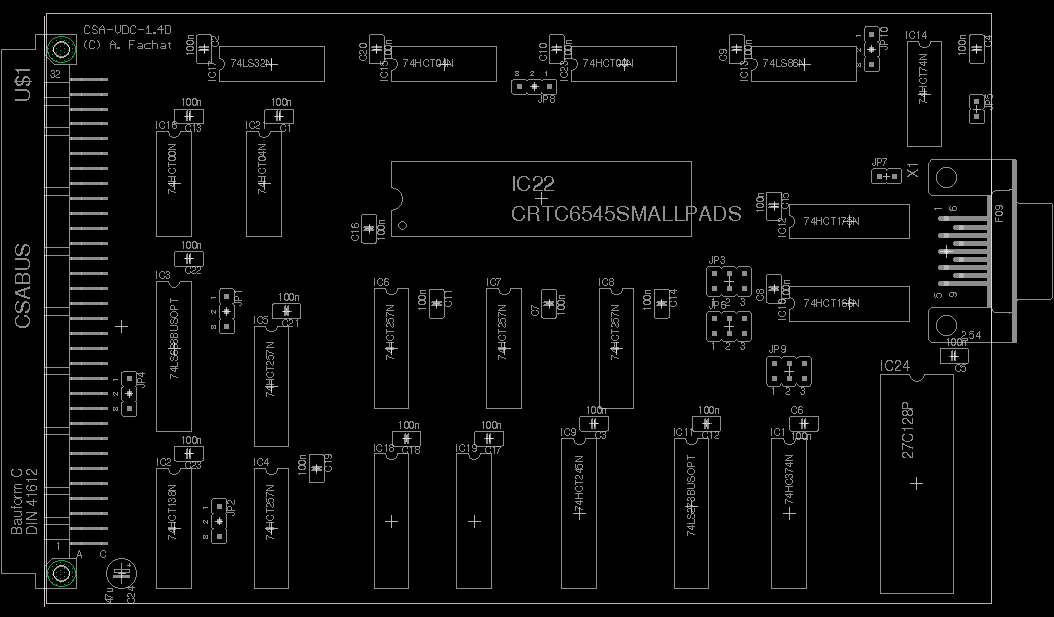
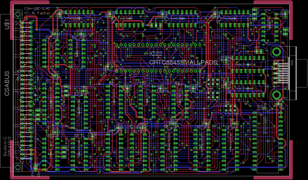
Version: 1.4D
Status: ok
Notes
| With a new monitor I noticed that the display enable was about half a pixel off, giving ghost artifacts on the right side of the screen from characters displayed on the left side of the screen. So I had to fix the timing for the DE latch. | |
| This layout is mostly tested (as a patched 1.4C) | |
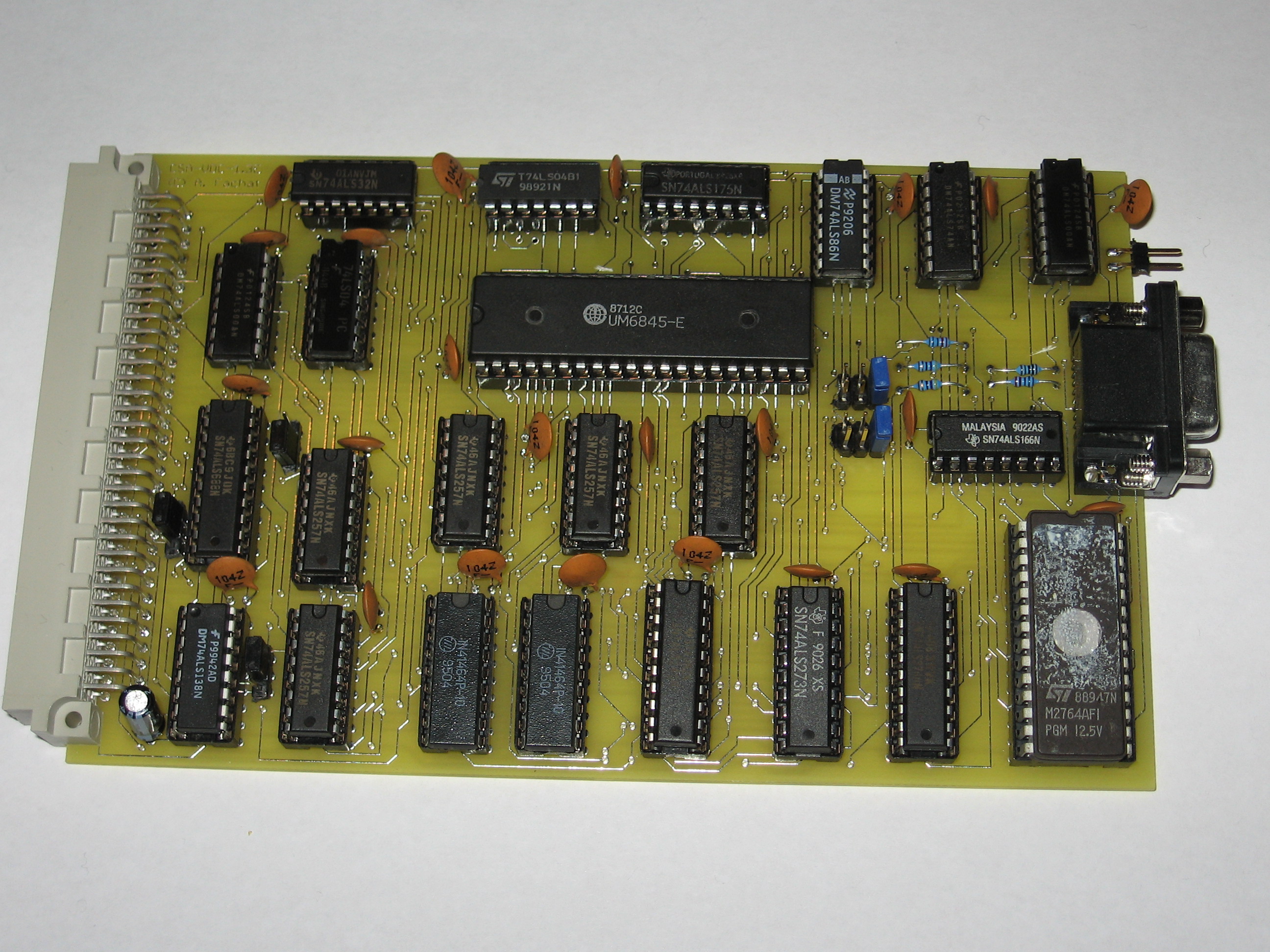
| In my current setup I have reused my 20 year old original video board (which wasn't working anymore). So all timing relevant ICs are 'LS technology ('LS04, 'LS00, 'LS74, 'LS257, 'LS32, 'LS138, 'LS86, 'LS175, 'LS166). The only exceptions are a 'HCT688 and a 'HCT245. Maybe I've finally defeated the dRAM timing hell here.... |
Version: 1.4C
Status: ok
Notes
| When testing my 1.4B version, I found a missing trace (bummer!), and I found that in different slot positions the display would be stable in others not. I found that the '74 latch was latching a signal (//Phi2) with the same signal transition as the latch trigger (8Phi2) - so I exchanged the 8Phi2 and /8Phi2 inputs on the IC14 clock inputs, and also used 8Phi2 instead of /8Phi2 on the pixel shift register clock. Now produces stable results in all slots. | |
| This layout is mostly tested (as a patched 1.4B) | |
| In my current setup I have reused my 20 year old original video board (which wasn't working anymore). So all timing relevant ICs are 'LS technology ('LS04, 'LS00, 'LS74, 'LS257, 'LS32, 'LS138, 'LS86, 'LS175, 'LS166). The only exceptions are a 'HCT688 and a 'F245 (which contrasts with the 'LS statement on 1.4B...). Maybe I've finally defeated the dRAM timing hell here.... |
Version: 1.4B
Status: untested
Notes
| The board has an improved layout on the 1.4A board, in that it has decent GND and VCC supply networks. Also it removes the delayed /CAS input to /RAMWE, as this was a bug. The board also got a jumper to set the external graphics character mode (for the PET emulation) via control register. The input to IC14A is inverted, to avoid jitter in the SR load line (adds an inverter from IC15 into the input line) | |
| This layout is untested. | |
| Most of the TTL chips are 'ALS technology, but a few have to be 'LS for timing requirements: IC9 is a 74LS245 so that the data read from the RAM is held on the bus longer, as the CPU requires a certain hold time of that data. IC21 is a 74ALS14(!) so that the delay between /RAS and /CAS is still long enough. IC9 may probably be an 'ALS04 as well, but never change a running system... IC15 is a 74LS04. |
Version: 1.4A
Status: untested
Notes
| In addition to the timing bugs this board implements a larger character ROM - now the character can be more than 8 pixels high. Also the crude circuit for the generation of the composite video signal is gone. Instead the video connector has an additional supply voltage pin, so the video plug can implement any better composite generation. | |
| This layout is untested. | |
| Most of the TTL chips are 'ALS technology, but a few have to be 'LS for timing requirements: IC9 is a 74LS245 so that the data read from the RAM is held on the bus longer, as the CPU requires a certain hold time of that data. IC21 is a 'LS so that the delay between /RAS and /CAS is still long enough. IC9 may probably be an 'ALS04 as well, but never change a running system... |
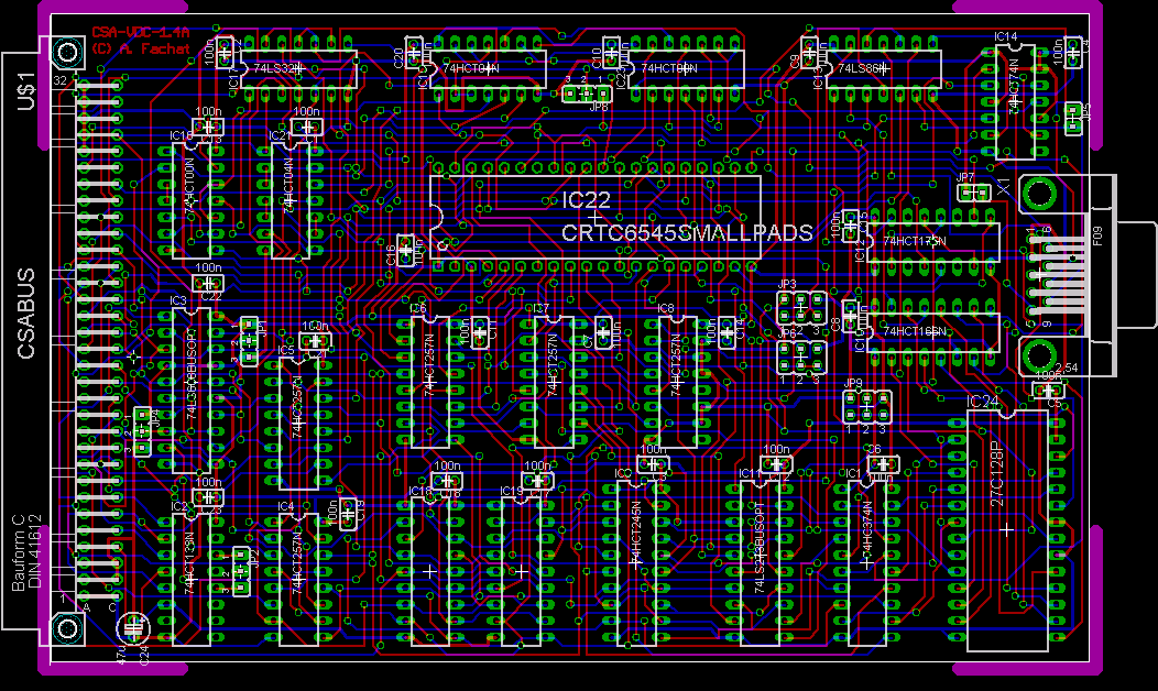
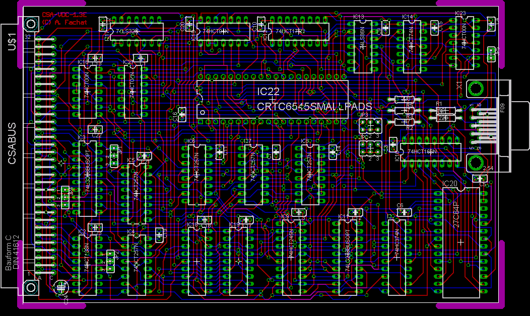
Version: 1.3E
Status: prototype
Notes
| This board version is a redo of the original board, with the known bugs fixed. | |
| During testing with the PETCPU and new CS/A board - with 74ALS technology I decided to better restrict the timing on the video board (which was not the cause of the problem), so I patched the board. The results can be found in version 1.4. |
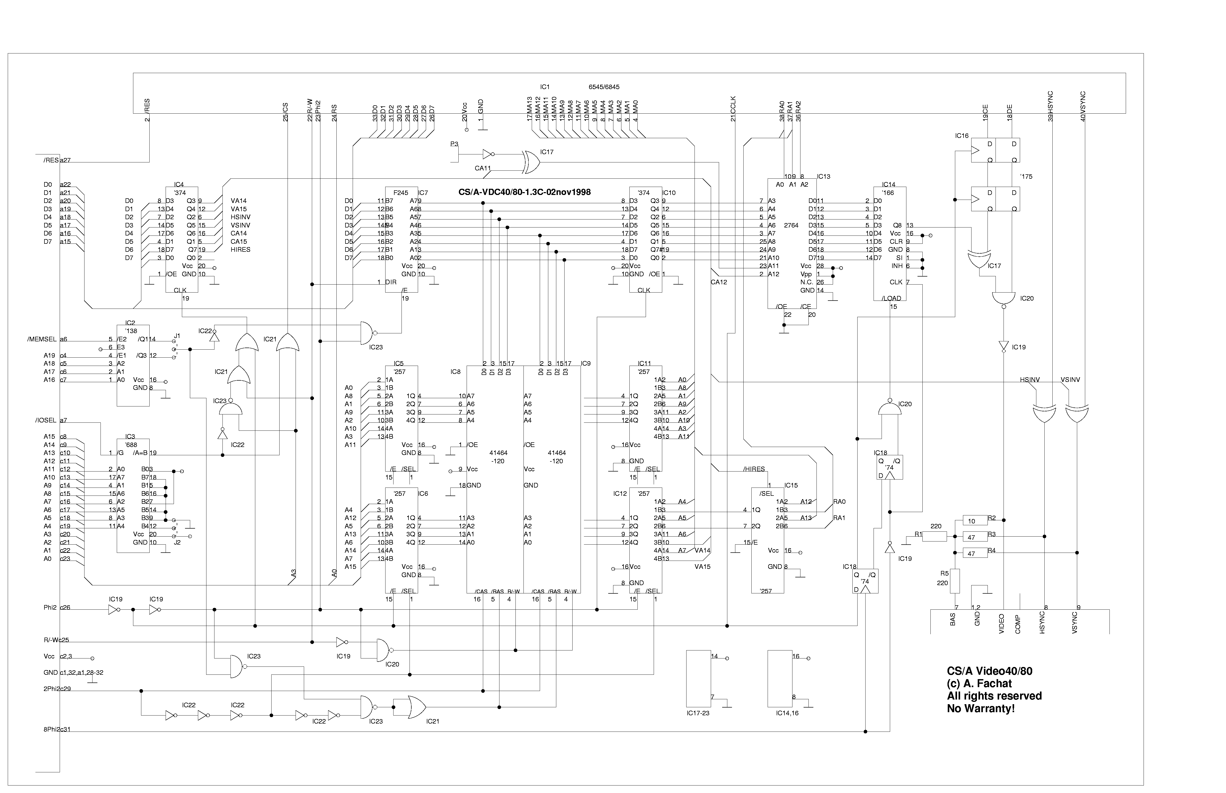
Version: 1.3C
Status: prototype with bugs
Notes
| This schematics has a bug in the circuit to generate the shift register load signal. It went unnoticed as my prototype board was manually soldered. |
Version: 1.3A
Status: prototype
Notes
| Scanned schematics only. Same bug as 1.3C. |
Files
| csavdc-1.3A-schem.png |
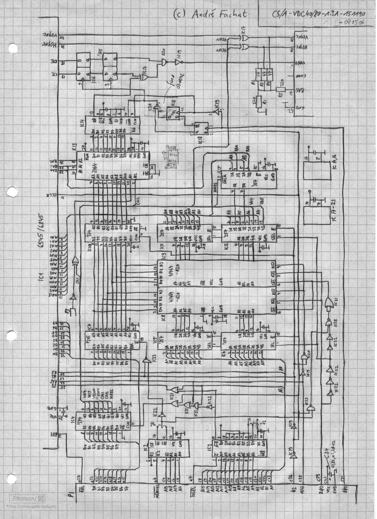
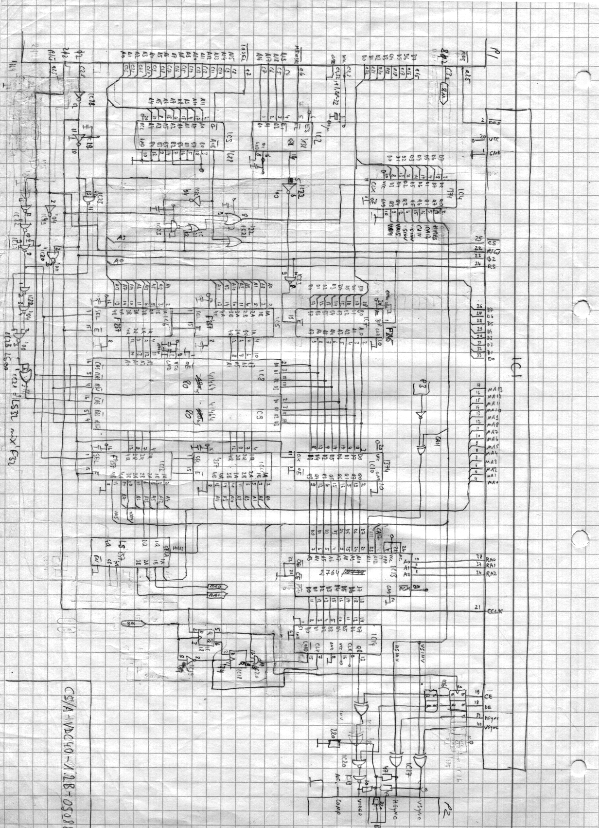
Version: 1.2A
Status: prototype
Notes
| This is the original video board. | |
| Scanned schematics only. Same bug as 1.3C. |
Files
| csavdc-1.2B-schem.png | |
| csavdc.jpg | |
| csavdcflip.jpg(The flipside - just for the fun of it... :-)) |
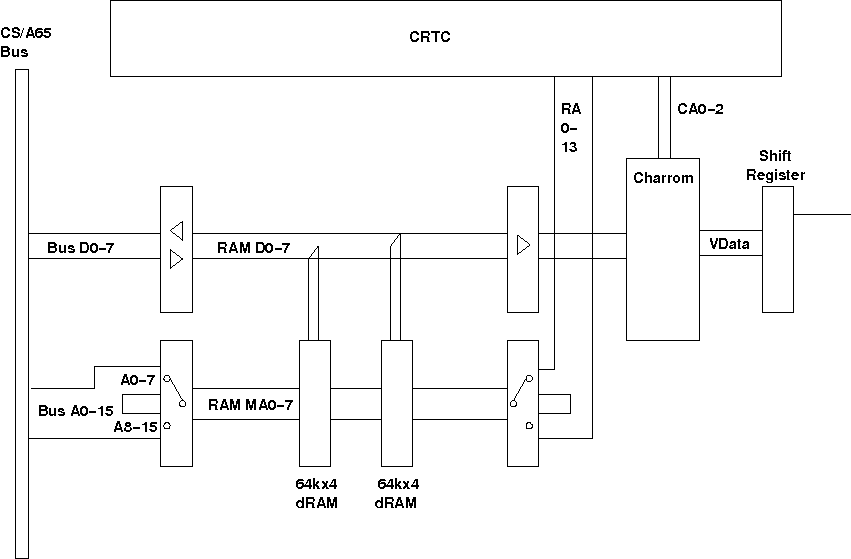
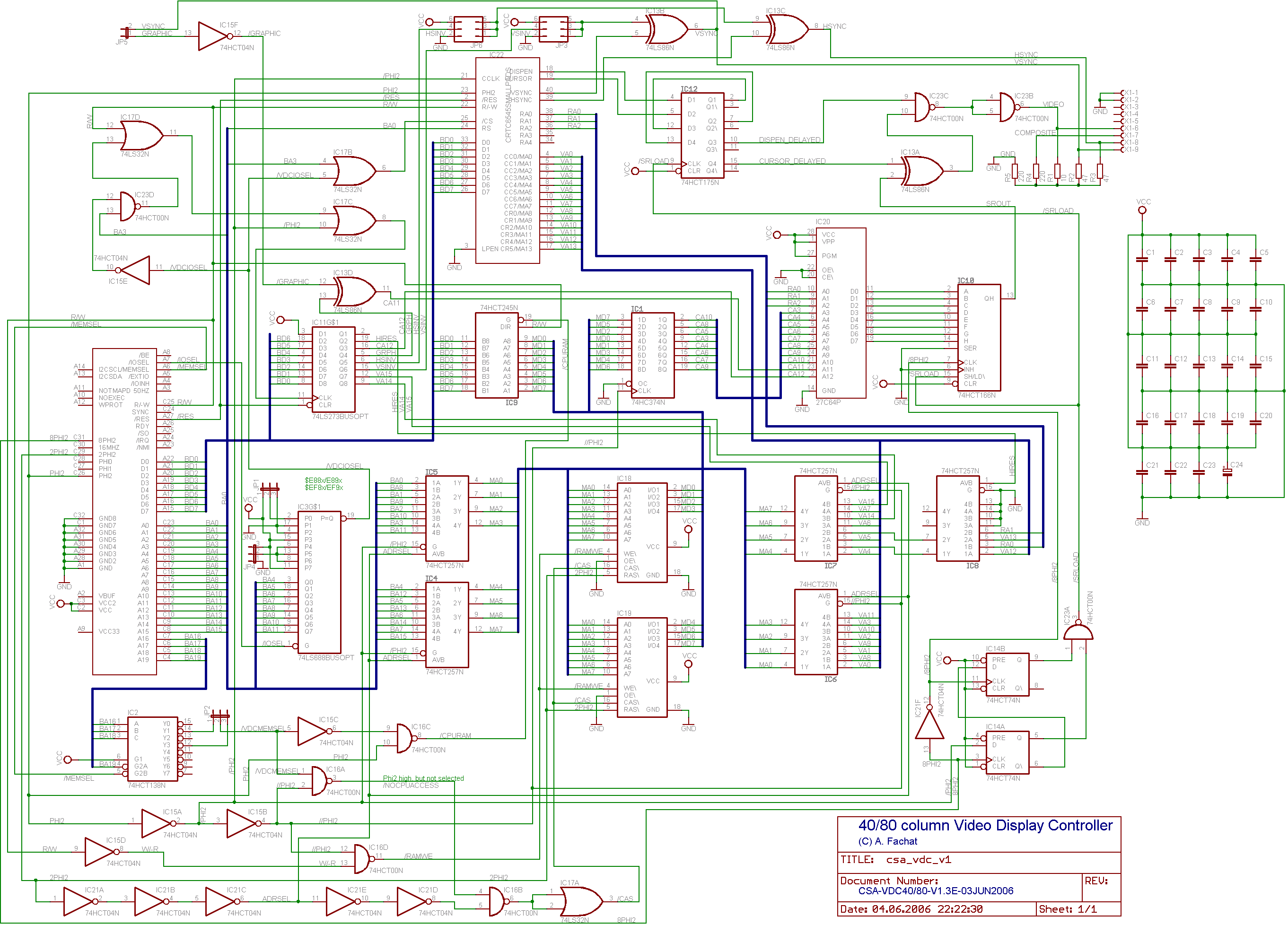
Block diagram of the vdc board. Only some relevant info
is shown. It is actually a pretty simple design, if
it were not for the timing...
The CPU accesses the memory during Phi2 high, so
then the BUSA0-15 and D0-7 are connected to the
memory address and bus lines. During Phi2 low the
video accesses the memory and thus RA0-13 is connected
to the memory. The byte read for the video is latched
and given to the character ROM as input. The CA0-2
lines select the correct scan line of the character
in the character ROM. The output of the character ROM
is then shifted out to the video output.
More on how the CRTC works can be found on the
CRTC page.