CS/A65 SPI Interface
This page is actually not about a complete board, but it documents the ways I use to connect SPI devices to the 6502. The first part actually is the interface to the SPI interface of MMC and SD-Cards.
- 2013-01-13 Added a new revision - this time using the VIA shift register - YES it is possible! - to access the SD card.
- 2011-03-06 Moved the SPI description from here to the SPI page.
Table of content
In a 6502 system several issues have to be considered:
Operating Voltage
The MMC and SD-Cards can operate with different operation voltages, but not with voltages as high as 5 Volt.
Fortunately I had, with my new PWR board, a 3.3V power supply I could use. Doing the signal voltage conversion was more difficult. As shown on USB-based Atmel/AVR Programmer: Level Converter, a 74VHC04 could be used to handle 5 Volt inputs even when powered with 3.3V - and giving 3.3V to the output. This IC, however, is SMD and hard to get, so I went for the slower (in terms of operating frequency) solution with open collector drivers as you can see in the schematics.
Fortunately the MMC boards are CMOS devices, and CMOS devices have a higher "high level" compared to standard TTL (see for example Logic Voltage Thresholds for TTL, CMOS, ...). Thus an output of a 3.3V-driven CMOS IC can still drive 3V, which for a 5V TTL chips easily is a high level. Therefore a 74LS* IC should suffice. According to the Level converter page above I successfully used a 74HCT family IC.
SPI Mode
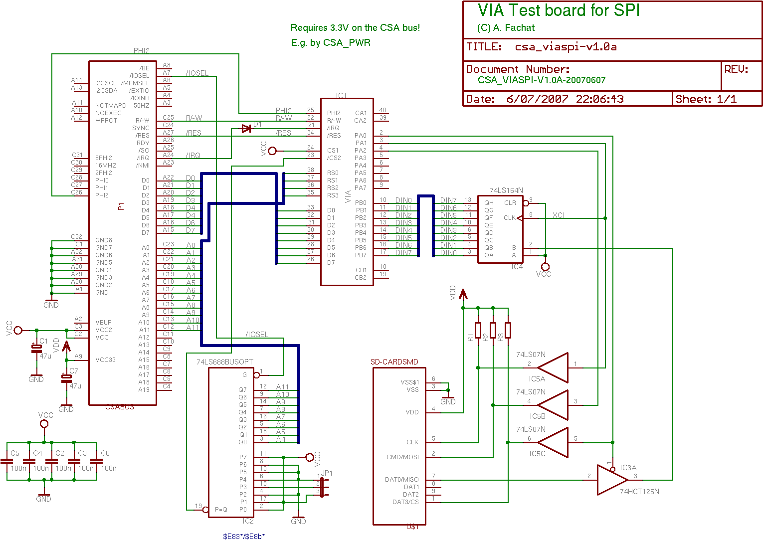
The MMC and SD-Cards operate with SPI mode 0. First I thought I could use the VIA 6522 shift register (SR) to handle the SPI port. As it turned out, however, the VIA SR transfers data out at the first (falling) transition of its clock, so it can be latched by the second (rising) edge by the receiver. This would be SPI mode 3. You could reverse clock, but you cannot make the VIA shift our earlier. So - I thought - there is no way to use the VIA SR. Instead in version 1.0 I used a bit-banging approach with CLK and MOSI.
For MISO, hoever, I decided to use an external shift register. This approach seemed to make sense with the VIA SR, as transfers work in both directions at the same time. Now it is just a convenience.
Shift register magic
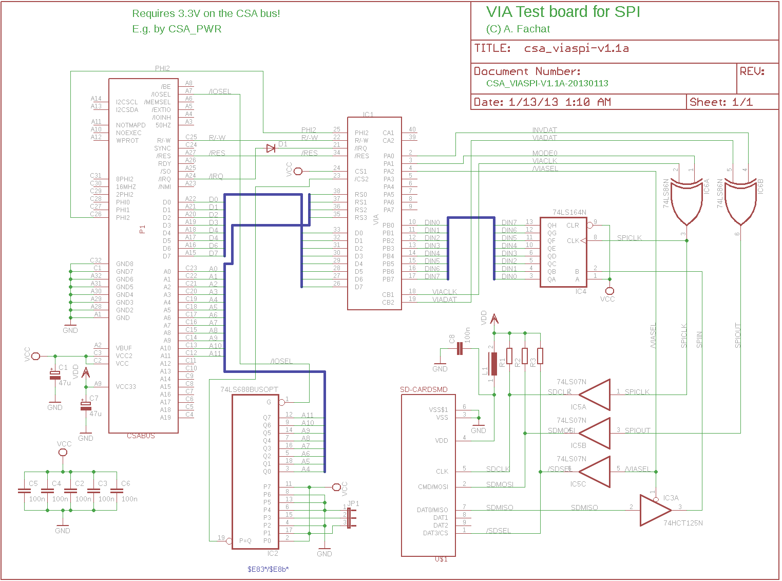
For release 1.1 of the board I decided I would take on another try of using the VIA shift register. And indeed I found a neat trick, that only needed an extra IC.
The VIA shift register with CB1 as clock output and CB2 as data output directly implement SPI mode 3. Inverting the clock could make that an SPI mode 1. However, for SPI modes 0 and 2, not only need the clock be inverted for mode 0, the first data bit needed to be available already before the start of the first clock pulse! The VIA cannot give this signal. So I though about setting the data line with the first bit manually. And that is actually easy with an extra XOR. The VIA keeps the data output CB2 as the last valid bit of the previous shift, i.e. bit 0. Make sure the last bit of every shifted data is zero, then invert the data line when the highest bit of the new data is set, and shift out the rest of the data.:
SD_SENDBYTEW
        ; mode 0
        ; make sure last bit is 0, shifting bit 7 into carry
        asl
        bcs invert
        ; last bit was 0, nothing to do but send the byte
        sta SD_VIA+VIA_SR
        ; wait to finish
        lda #%00000100
wait0   bit SD_VIA+VIA_IFR
        beq wait0
        bne end

invert  ; invert the current bit (which is last bit from prev.
        ; data byte, which we set to zero
        inc SD_VIA+VIA_DRA
        ; compensate for the inversion
        eor #$fe
        ; send out the data
        sta SD_VIA+VIA_SR
        ; wait to finish
        lda #%00000100
wait1   bit SD_VIA+VIA_IFR
        beq wait1
        ; reset inverter
        dec SD_VIA+VIA_DRA
end     ; clear int
        sta SD_VIA+VIA_IFR
        ; read read data
        lda SD_VIA+VIA_DRB      ; load from external shift reg
        rts
This way the VIA can actually do SPI mode 0!
Note: I kept it simple. This schematics can only do mode 0 and mode 3. If I had to enable mode 1 and 2, then the inverter for the clock need to be separated for an inverter for the clock going to the SPI bus, and an inverter for the input shift register. Why that is is kept as excercise to the reader.
OS/A65 SPI driver 1.1
This is a test driver for the SPI 1.1 schematics below. I uses the VIA shift register to access the SD card.
It initializes the card, reads the operations conditions register, the card id data, and can read and write a block.
Please note that it is clutterd with debug code.
Also note that the driver is "conservative". It actually waits even when sending a byte, to undo the inverter. It could just "fire-and-forget" and check on the next call whether the previous byte is done.
OS/A65 SPI driver 1.0
This is a test driver for the SPI 1.0 schematics below. It initializes the card, reads the operations conditions register, the card id data, and can read and write a block.
Please note that it is clutterd with debug code.
Version: 1.1A
Status: prototype
Notes
| I have built this schematics on a prototyping board, so there is no board layout for it. | |
| This approach uses the VIA shift register, which allows you much faster speed than bit-banging! | |
| For hot-plugging a capacitor and inductor have been added in the power supply lines for the card (this is untested though). |
Version: 1.0A
Status: prototype
Notes
| I have built this schematics on a prototyping board, so there is no board layout for it. | |
| You may not need the input shift register. This is not really necessary if you bit-bang the input as well. It is convenient, however, and a remainder of an earlier approach using the VIA shift register (which did not work unfortunately). | |
| For hot-plugging another capacitor may be needed in the power supply lines for the card. |