CS/A65 RAMDisk
This board uses the (now outdated) 30-pin SIMM memory modules to build a RAM disk with up to 16Mbyte. The memory is accessible via a single register, using an auto-increment byte address counter (8-bit byte address within page only).
Two major board versions are available. The first one is more a concept and is built from TTL logic glue. The second one uses a CPLD to implement the DRAM controller.
The CPLD board is brand new and undergoing tests. With version 2.0E the power glitch has been fixed - the '245 driver was activated too early so it reached into the previous refresh cycle. The board works stable at 1MHz bus frequency, with 4 DRAM modules. At 2MHz write timing is stable, but there are read glitches (repeated reads vary). On the scope the signals look fine, from timing and shape, and seem to work for writing, so I am investigating bus terminators for the main system bus now.
The current status of the TTL board is that it works in some specific configurations. I built the board over two years ago and encountered a number of errors (see notes below). Only recently I have tested it with the 65816 CPU board, where it works with 3 modules with 1MByte each, but not 4 modules. I still have to retest with other CPU boards and 3 modules only.
Further tests still have to be performed, but I am not sure how far I will go into this with this design version. I had a discussion with Bil Herd - yes, the designer of the Commodore 128 - who suggested some improvements:
The new CPLD-based ramdisk board.
- Use a state machine and a GAL to create a simple DRAM controller and not rely on gate delay times to create signals. I found the 8296 timing signal generation a good example for such a system.
- The board layout used could use some improvements in the layout of the power supply lines, but also the address and data lines.
- The board lacks series resistors, and termination resistors, so signal reflections could easily be a problem.
- The /RAS signal is always sent to all modules - on a CPU read or write cycle only the active module needs it. This could be a reason for the problems below, which are possibly power supply related and if all modules draw power at the same time the actual access might fail.
- Maybe even use an FPGA to implement a DRAM controller
See the this page for the full discussion
The CPLD-based design for this board reflects these discussions.
Table of content
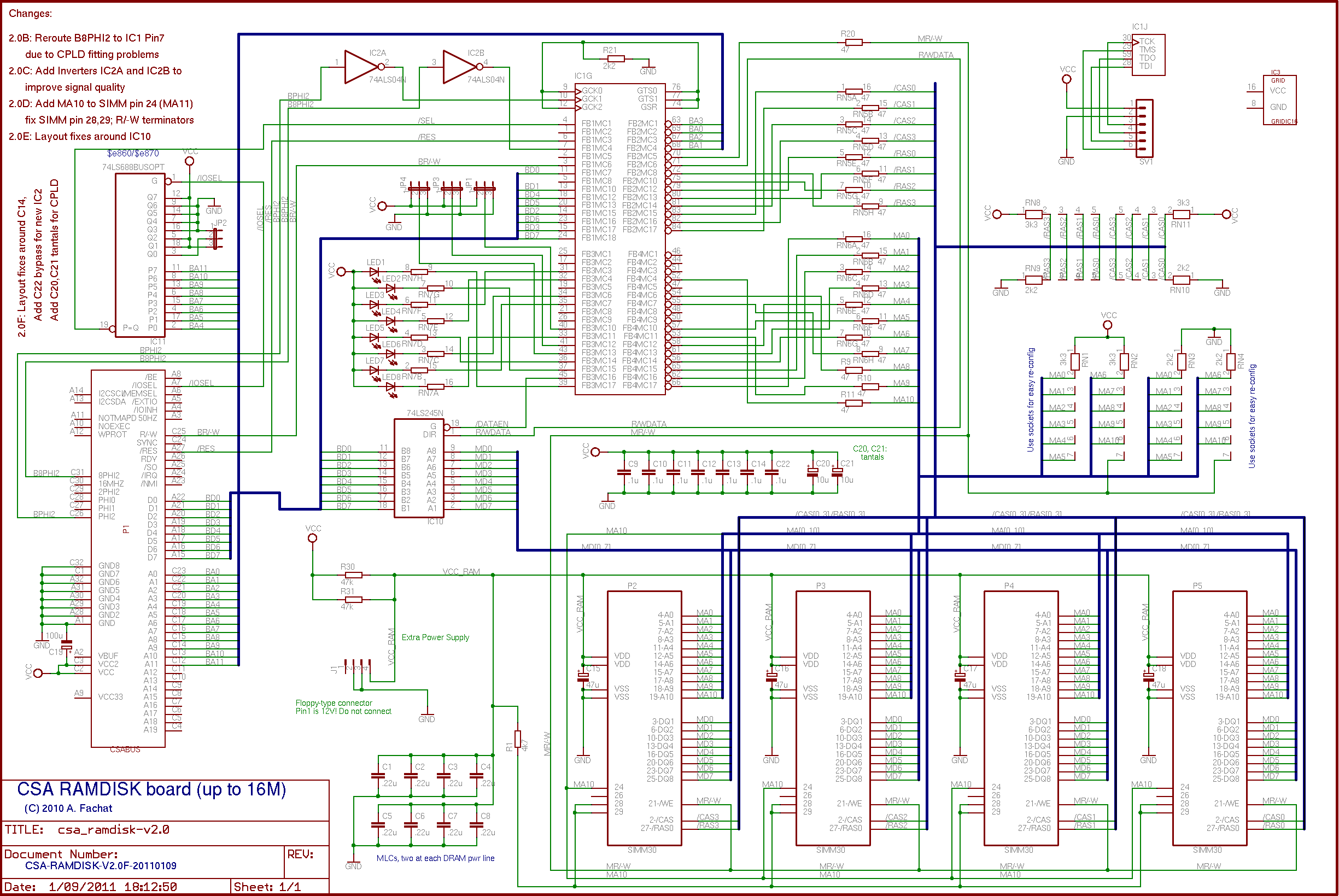
Version: 2.0F
Status: prototype
Notes
| This improves on the 2.0E version by adding more bypass capacitors, esp. the one for IC2 that was missing. Two of them are tantals and the CPLD supply voltage is routed over them in the layout. | |
| The VHDL has some timing improvements. The 2.0E was still producing a heavy jitter on the power signal, which is now gone. |
Files
| csa_ramdisk-v2.0f.sch | |
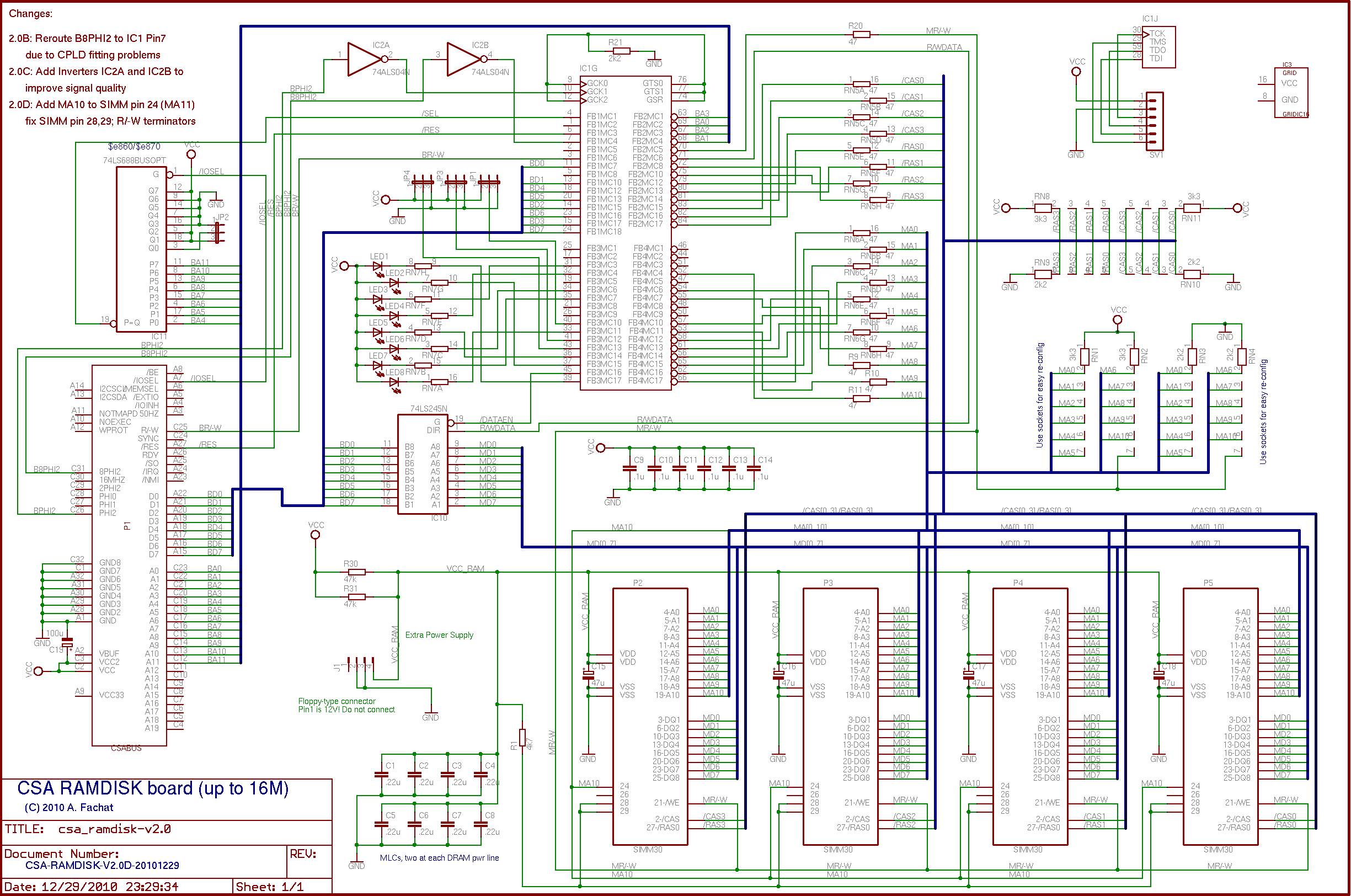
| csa_ramdisk-v2.0f-sch.png | |
| csa_ramdisk-v2.0f.brd | |
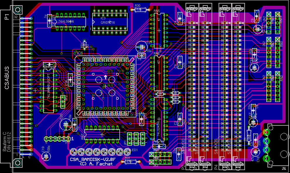
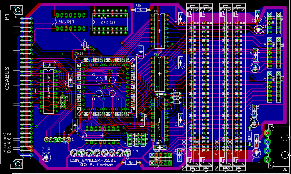
| csa_ramdisk-v2.0f-brd.png | |
| dramctrl-v2.0f.vhd(CPLD VHDL source) | |
| dramctrl-v2.0f.ucf(CPLD constraints file (pin mapping)) | |
| dramctrl-v2.0f.jed(CPLD compiled source) | |
| ramdisk-tests.tar.gz(Test programs) |
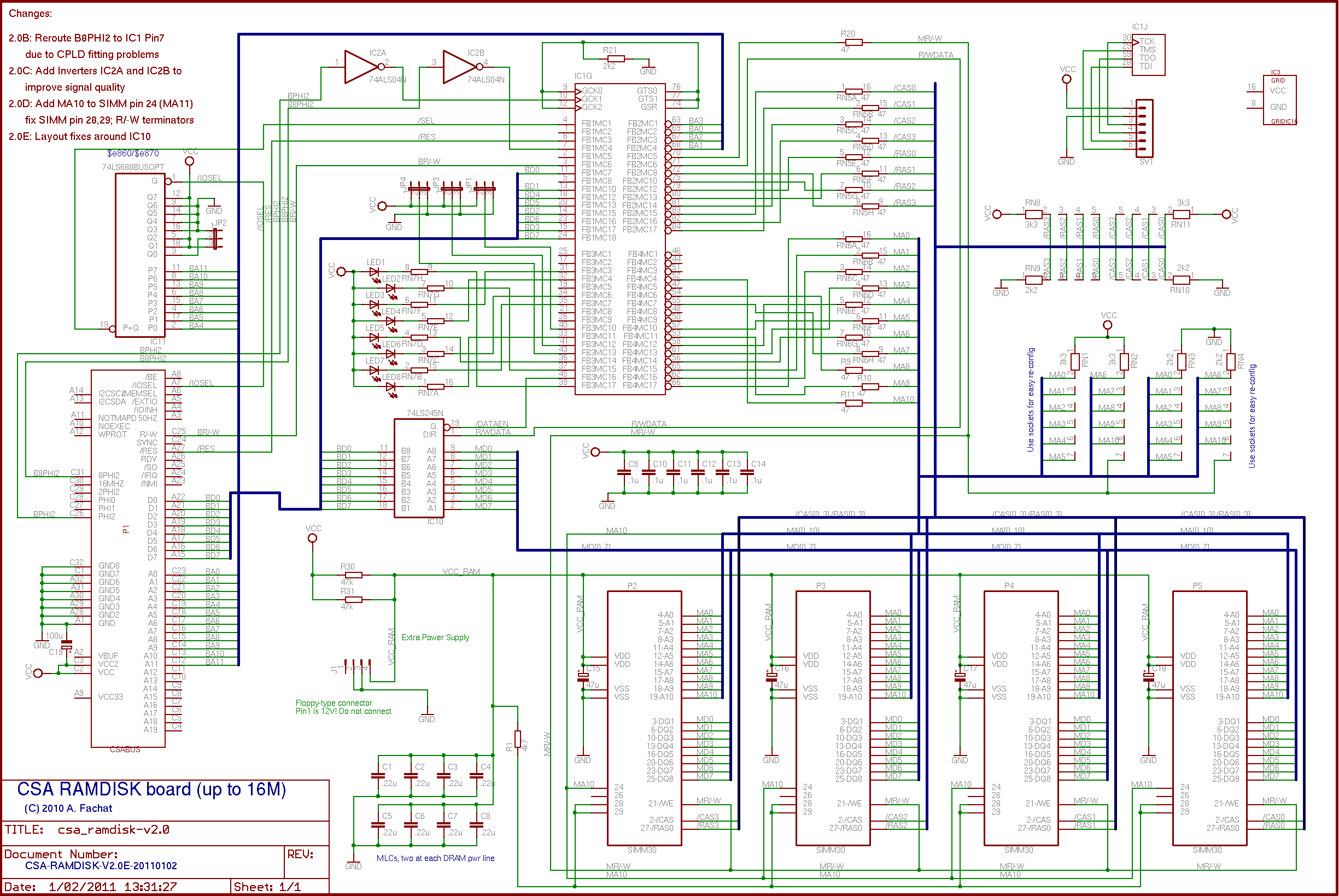
Version: 2.0E
Status: prototype
Notes
| This board works stable at 1MHz system bus frequency, tested with up to 4 modules with 1 MByte each. | |
| I currently use 4k7 Ohm terminators both to GND and to VCC. | |
| Compared to the 2.0D it has only a small layout fix (so the GND for the '245 driver is routed directly to its bypass cap, not closer to the DRAM GND... The CPLD has fixed timing, and some glitch prevention from the main bus. The '245 can now be 'LS or 'ALS. |
Files
| csa_ramdisk-v2.0e.sch | |
| csa_ramdisk-v2.0e-sch.png | |
| csa_ramdisk-v2.0e.brd | |
| csa_ramdisk-v2.0e-brd.png | |
| dramctrl-v2.0e.vhd(CPLD VHDL source) | |
| dramctrl-v2.0e.ucf(CPLD constraints file (pin mapping)) | |
| dramctrl-v2.0e.jed(CPLD compiled source) | |
| ramdisk-tests.tar.gz(Test programs) |
Version: 2.0D
Status: prototype
Notes
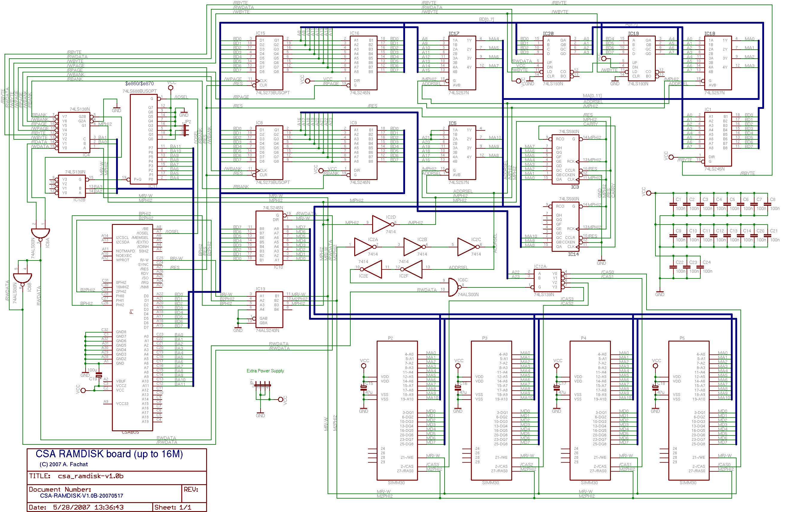
| This is a complete redesign - using a CPLD instead of a set of TTL logic glue. Also it now adds - by design - series and termination resistor networks to improve signal quality. | |
| The /CAS, /RAS, and DRAM address lines have series as well as termination resistors. I found that the terminator combination in the schematics (2k2/3k3) seems to draw a lot of current from the CPLD. I currently use a 4k7 terminator to ground, but none to VCC. | |
| I've tested the board with three types of SIMM modules. One is a three-chip low profile module with parity (which isn't used), one is an industry module with nine separate SMD memory chips (i.e. also with parity), and the third one is simple board where I soldered eight separate chips (through hole). All modules have 1MByte (although I thought the three-chip module would be 4MByte, I cannot remember giving this one away, just as I cannot see a defect in the address decoding). | |
| The '245 bus driver MUST be an 'LS type, not an 'ALS. If you use an 'ALS, it somehow at some point seems to drive against the DRAM while reading. I found ripples of up to 550mV on the power supply lines on both(!) sides of the board (bus power supply and external power supply) when using the 'ALS type. Even when the external power supply was regulated out of a 12V that did not show those ripples. Shortening the active period (/EN) for example by masking the signal with RAS helps with the power ripples - but makes the data unreliable. The 'LS seems to work fine so far. |
Files
| csa_ramdisk-v2.0d.sch | |
| csa_ramdisk-v2.0d-sch.png | |
| csa_ramdisk-v2.0d.brd | |
| csa_ramdisk-v2.0d-brd.png | |
| dramctrl-v2.0d.vhd(CPLD VHDL source) | |
| dramctrl-v2.0d.ucf(CPLD constraints file (pin mapping)) | |
| dramctrl-v2.0d.jed(CPLD compiled source) | |
| ramdisk-tests.tar.gz(Test programs) |
Version: 1.0C
Status: buggy
Notes
|
With the 65816 CPU board the RAMDisk has been tested
and found working for up to 3 modules with 1MByte each.
With 4 modules certain RAMDisk addresses do not seem
to work properly. Tests with larger modules (4M) still have to be performed. | |
This is the current set of errors. The spurious counter pulses seem gone: 1) I wrote some test programs (not yet very sophisticated, but working The programs work (so far) in the lowest 64k of the RAMDisk. What I found out that there are only two addresses in a page, that give problems - $45 and $65. And that only on some of the pages, pages $1x, $5x, $9x, $dx. Interestingly the two addresses have different problems:
I don't yet know what to make of that, though. The bit pattern don't make sense to me, esp. address bits 12/13 (that seem to have to be fixed to 1/0 to give problems) and bit 5 (that seems to give problems) are handled in different ICs. 2) I scoped the supply lines for the ICs and the DRAM modules. I found a jitter of up to .3 Volts on each line (GND and VCC). So I added a .1uF multilayer capacitor to the 'LS257 that generate the multiplexed RAM address lines, and a 1u MLC in parallel to the already existing capacitors in the DRAM supply lines. The jitter did not improve much, although I had one effect: before adding the caps the problems mentioned above in 1) were also seen in addresses $47 and $67, and sometimes $44, $48, $64 and $68 - which is fixed now. | |
| I have created this board by modifying the 1.0A board. Currently no layout is available. |
Version: 1.0B
Status: buggy
Notes
| The board timing is not yet fully working. | |
| This board currently has a problem with the counter on read accesses. Spurious read strobes appear that increase the counter on read accesses (but not on write accesses). I do not yet have found the source of this problem. |
Version: 1.0A
Status: buggy
Notes
| The board timing is not yet fully working. | |
| This board currently has a problem with the counter on read accesses. Spurious read strobes appear that increase the counter on read accesses (but not on write accesses). I do not yet have found the source of this problem. | |
| The board has a timing problem. The delayed 2Phi2 signal used with RWDATA by IC6C to generate the input to IC12A comes to fast. This is fixed in V1.0B. | |
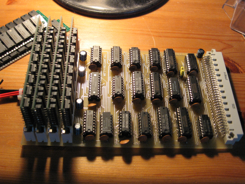
| The dynamic RAM draws a lot of power. The CSA PWR board checks the supply voltage, so if this board is plugged in, the supply voltage drops below the RESET watcher threshold, and /RESET is asserted. V1.0B contains an additional power supply plug. |
Files
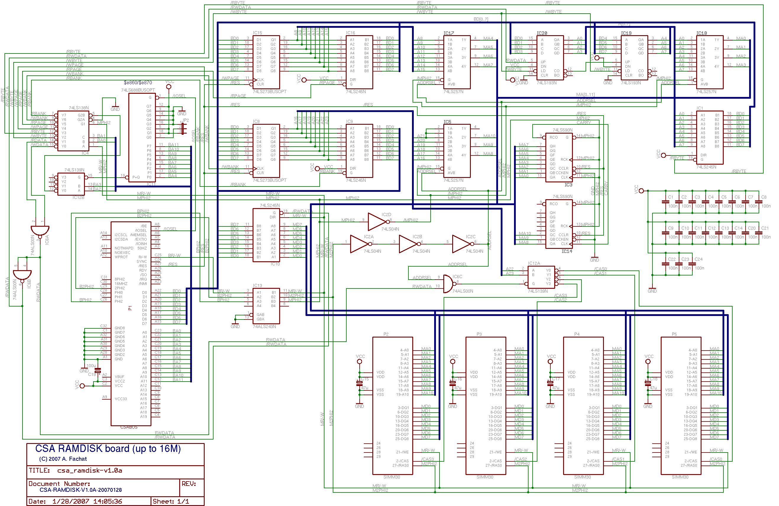
| csa_ramdisk-v1.0a.sch | |
| csa_ramdisk_v1.0a-sch.png | |
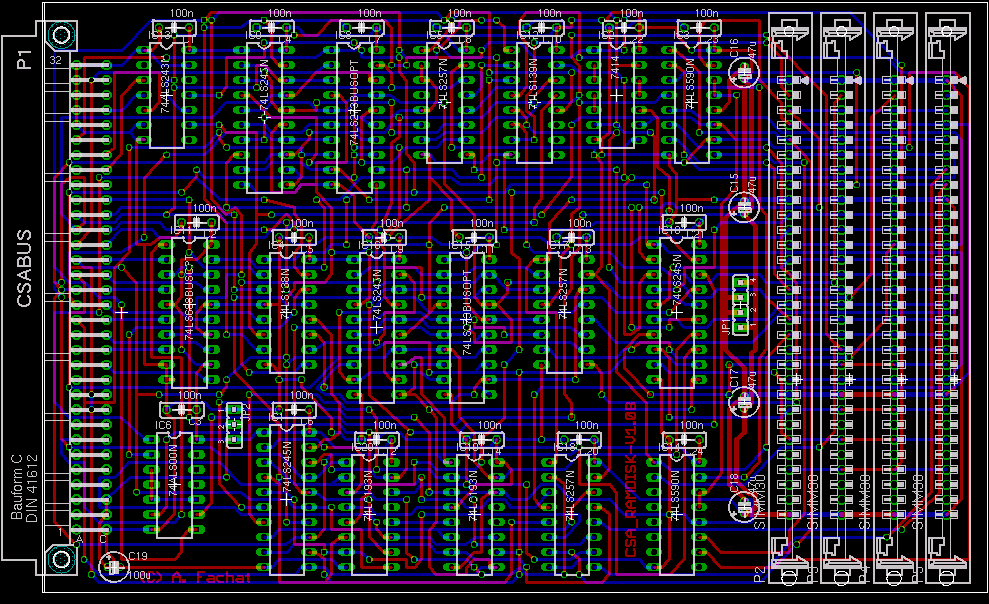
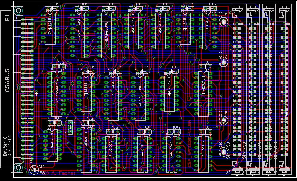
| csa_ramdisk-v1.0a.brd | |
| csa_ramdisk_v1.0a-brd.png | |
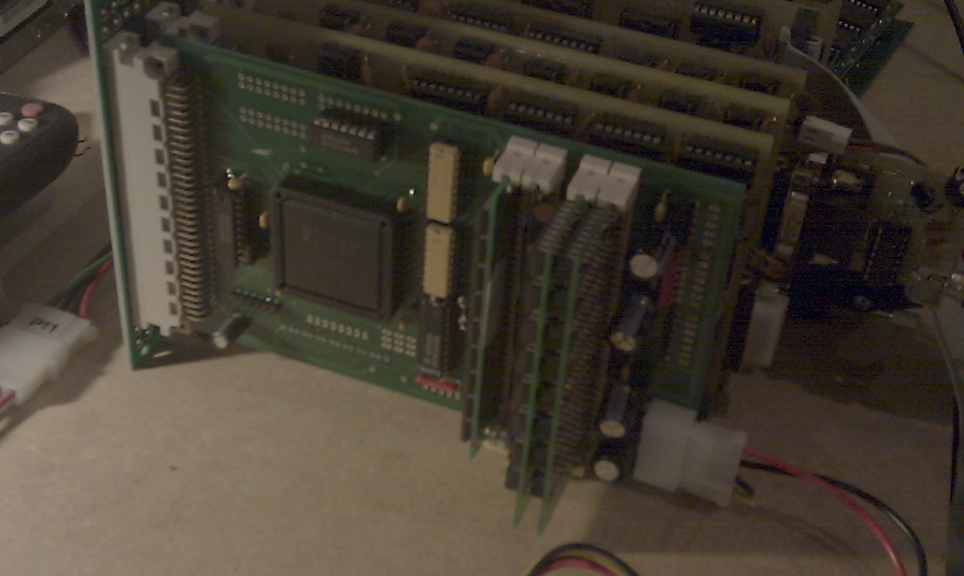
| ramdisk_v1.0a-1.png(On the left you can see the floppy-type power connector cable I soldered to the bottom) | |
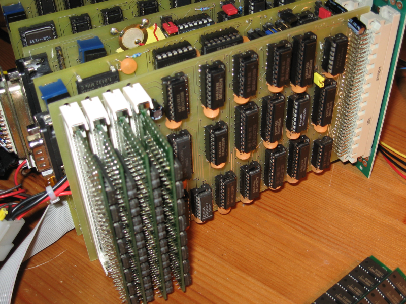
| ramdisk_v1.0a-2.png |