The 65k Project - Architecture Overview
(C) 2010-2011 André Fachat
This page describes an overview on the 65k architecture.
- 2012-04-11 Moved and updated to 65002R0
- 2010-10-23 Published this page
- 2010-10-14 Started this page
Table of content
License
This content is licensed under the Creative Commons Attribution Share-Alike license, CC-BY-SA version 3.0.
Note this "content" includes this web page, but does not include the 6502.org header and the left and right web page columns. Click on the "Maximize" link to see the contents covered by this license.
Disclaimer
The content comes with no warranty at all! There is no guarantee and no promise that this specification is correct, consistent, will actually work, or will ever be implemented at all.
To my understanding the techniques described here have been used by various processors for decades already. Still there is no guarantee that a processor according to this spec would not be covered by some patents.
Subject to change without notice!
Contributors
- André Fachat - initial author: 8bit Homepage
Changes
This section describes the changes to the document:
| Date | Author | Changes |
|---|---|---|
| 2010-10-25 | André Fachat | Updated Core Architecture Diagram and Description |
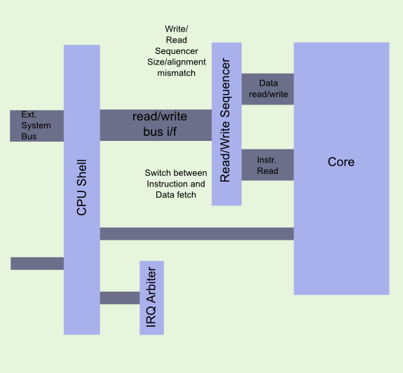
This section describes the top level architecture, i.e. the top level building blocks of the processor and their relations. Compared to the 6502 there are more such building blocks, the processor is more complex. The 6502 basically compares to the core - which is described in more detail below.
The following sections describe the components.
Core
The core is the actual processor. It contains registers, ALU, and so on. With the rest of the system it communicates using three bus interfaces:
- Instruction fetch bus - read the next instruction
- Data read bus - read some data word
- Data write bus - write some data word
Read / Write Data Sequencer, Read Arbiter
The read and write sequencers break down misaligned memory accesses into accesses that can be executed on the external bus. The core has two channels to the read/write sequencer - one for data reads and writes, one for opcode fetches.
The read/write sequencer is adaptable and prepares for and accepts read/write transfers in any bus width available. I.e. you can connect byte wide, word wide or long wide memory. The core provides write data such that each type of memory gets the data on the correct bits. Depending on the address offset the memory has to actually overwrite only the changed parts. For example:
| Write width | Address offset | Output | ||||||||||||||||||||
|---|---|---|---|---|---|---|---|---|---|---|---|---|---|---|---|---|---|---|---|---|---|---|
| 8 | 3 |
| ||||||||||||||||||||
| 16 | 1 |
| ||||||||||||||||||||
| 16 | 2 |
|
Note that the address offset is the lowest two bits of the address (for up to long memory access, quad access would need the lowest three bits) - depending on the requested access width and the address offset the attached memory must only overwrite the valid data to be written (i.e. create the select/write enable signals). The attached memory then signals the memory width to the read/write sequencer, which increases the address and determines if a second (or more) access is required.
For read accesses, the attached memory signals the access width to the core, and the read/write sequencer picks the right bytes from the input signals. It then updates the address accordingly depending on attached memory width and address offset, and checks if the access is done.
In the read/write sequencer the data read/write accesses take precedence over the instruction fetches. Another difference is that the data read/write accesses are broken down from the requested width to the memory access width, and accesses are done in sequence until the full data has been transferred. The fetch access always requests full width - but accepts chunks of data in all width, just as they come in.
CPU Shell
The CPU shell passes the memory accesses to and from the read/write sequencer. If the system had mulitple cores, the shell would select from which core the access would come from.
The CPU shell also handles the interrupt input signals, passes them to the interrupt arbiter, and then to the cores.
In the future it will also handle the processor configuration register handling.
IRQ arbiter
The IRQ arbiter receives the interrupt signals from the external interface and can distribute the interrupt signals the different cores.
The current version just routes all interrupts to the first core.
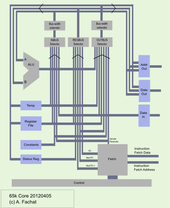
This section describes the architecture of the processor core. A block diagram is on the right side, click it to enlarge.
The general principle of the core is that every action takes one cycle, from falling phi2 to falling phi2. Within this cycle, the values from one or two registers (including data bus input for example) is transferred to another register, including address or data output busses.
Within the core there are registers, bus extenders, an ALU, a fetch logic, controller, and a bus interface. All those are described below. The components are placed around three busses, the "outbus" (main purpose: output from the ALU), the "inbus" (main purpose: input from the data bus) and the "regbus" (main purpose: output from a register). During the programming of the opcodes I found that I had to provide many more connections to avoid moving data around or adding extra temporary registers, so the three busses now have many more inputs than originally planned.
Registers
The registers are implemented in different components: A temporary register, the register file, a constant register file, and the status register.
The constant register is the most simple one, it just provides a number of constant values (e.g. to add or substract address offsets during address computation).
The temporary register stores, at falling phi2, the input value and presents it on the output.
The register file contains the A,X,Y,B,E as well as USP and SSP registers. It takes a read register number at falling phi2 and presents the contents of the register after the falling phi2. It holds the last value read even if the read register number drops. At the same time it allows to write any of the registers using the write register number. This synchronous operation allows to use block RAM in an FPGA (once I have figured out how to do this...) The USP and SSP registers behave differenly. Both are implemented twice, the original register and a fallback register that is updated when the opcode is finished. The reason is that in case of an abort the fallback register needs to be written back to the original register. This is done as part of the register file, not of the operation sequencer.
The status register contains the status bits. These bits are the same as in the original 6502, but add the u and x flags. The "u" flag is set in user mode and clear in hypervisor more. The "x" flag is used as part of the stack frame to signal an extended stack frame. Apart from the "usual" inputs to the status register e.g. from the ALU to set the flags, the status register has connections to the outbus and regbus to handle stack pulls and pushes of the status register. Similar to USP and SSP the status register flags are implemented as original and fallback to be able to correctly handle ABORT situations.
Note that only status, USP and SSP require ABORT handling.
Extenders
The bus extenders for the inbus and outbus allow extending values to the full bus width using zero-, one-, or sign-extension (or pass through the value). This is not only used according to the prefix bits, but also to extend the offset parameters for example.
ALU
The ALU provides the aritmethical and logical operations. Note that besides the ADC and SBC operations it also supports ADD and SUB that do not use the carry flag. Those are used for example in address computations. The ALU is asynchronous.
Fetch
The opcode fetch requests data from the read/write sequencer and stores it into the input buffer. Once it has determined that the input buffer contains the full opcode, this opcode is presented to the control sequencer until it is taken.
Meanwhile the fetch logic fills up the input buffer, so that subsequent opcodes can be fed directly from the fetch logic to the sequencer even without memory access.
In case of an interrupt the fetch logic injects an IRQ handling opcode into the opcode sequence. The same basically happens on ABORT, only that an ABORT is signalled by the control sequencer when a memory access problem ("seg fault") has been detected.
Control (sequencer)
The control sequencer takes the opcode from the fetch logic, and sequences it into control signals for all the other components. It stops counting when a memory access takes more than one cycle, so it handles the RDY stuff.
Now that the first revision has been made, there is need of some discussion.
Predecoding and register RAM
The control sequencer is implementing some prefetch logic for when the opcode is being taken from the fetch logic. Before the opcode is actually stored, it is used to compute a read register number to send to the register file, so that the register value can be used in the next cycle. This is done to allow the use of block RAM in the register file.
Although this predecode is already interleaved with the last cycle of the previous opcode, it introduces complexity and path length which reduces the overall clock frequency. It is not clear to me if it actually helps that much with the block RAM to justify this effort.
At one time this path was the critical path for the timing calculations.
Path length
The current version (as of april 11, 2012) has a maximum of 32 levels of logic and a clock limit of about 12 MHz when implemented in a 4ns Spartan 3. This is the result of a long path length, that also seems to be routed all across the CPU. I don't really understand those paths yet though. The paths that are shown in the tool's analysis should not exist...
Last modified: 2012-04-29

