PET index - Drive Architecture
(C) 1998-2018 André Fachat
The 5.25" disk drives (and possibly the 8" and harddrives as well) share the same architecture. In this page you find information about the architecture of these drives.
- 2018-12-29 Added the link to the GCR page
- 2010-01-04 Started this page
Table of content
The architecture is actually a quite elegant solution to wire two CPUs together, as well as it has an ingenious method of handling GCR data in hardware. The following block diagram shows this (click to enlarge):
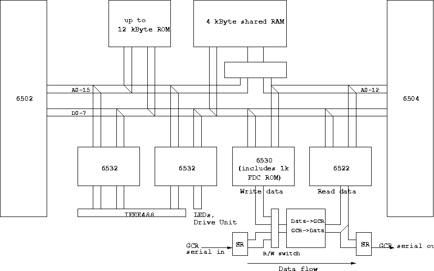
The two CPUs work on a phase inverted clock, i.e. when the 6502 has Phi2 active, the 6504 is has it passive and vice versa. The CPUs only use the data bus (approximately) during the active phase, so the data bus could be shared between the CPUs! The address bus is always active, so it canot be shared. For the shared RAM, the address bus is switched with the clock phases. Thus only the shared RAM, and nothing else is shared between the CPUs.
The DOS CPU has two 6532 as I/O interfaces. They not only provide the I/O, but also have 128 byte RAM each, that are used for the CPU's zeropage and stack. The I/O is mainly used for the IEEE488 interface, as well as the LEDs and the drive unit detection.
The FDC CPU has a 6530 and a 6522 chip for I/O. The I/O is used to control the drives. The VIA 6522 is for example used to control the motor and the head steppers.
Commodore disk drives store the data in GCR (Group Code Recording) format on the disks, which is different from the (IMHO inferior), nowadays used MFM encoding. I will not go into the difference, only note that in GCR, 4 data bytes are computed into 5 GCR bytes. In fact, 4 data bits are computed into 5 GCR bits.
Now when writing to the disk, the FDC CPU writes the data to the 6530. This data byte is split into two 4-bit nibbles, and each nibble is expanded by one bit. The low nibble gets the "mode select" as 5th bit, the high nibble gets a zero bit. These ten bits are then used as address input to the ROM. the 8 data lines from the ROM are also expanded: the ROM input A2 (former output data bit 2) is inserted as output bit 2, and ROM input A7 (former input bit 6) is inserted as output bit 7. I.e. for each original data nibble, bit 2 (value 4) is directly inserted in the middle of the resulting 5 bit GCR code. [Note: I have yet to understand why this is so, though... Maybe the GCR code used had this feature that one bit always was a certain input bit. Maybe the GCR code was selected that way to allow this mechanism...] The expanded 10 bit GCR data is now fed into a shift register and sent to the drive head.
When reading data from the drive, the serial GCR data is parallelized by a 10 bit shift register. This code is used as input to the same ROM as above (but with A10 switched, so different ROM content is selected). The output of the ROM is then read by the CPU.
To see the details of the GCR encoding look at the wikipedia page for GCR.
- GCR entry on wikipedia GCR encoding with list of GCR codes
The following table has been composed by William Levak:
                        4040 Memory Map
composed by William Levak

            6502                               6504

0000-007F  6532 #1 RAM            6530 RAM            0000-003F
0080-00FF  6532 #2 RAM
0100-01FF  6532 RAM shadows
0200-001F  6532 #1 I/O            6522                0040-004F
0220-027F  6532 #1 I/O shadows    6522 shadows        0050-007F
0280-029F  6532 #2 I/O            6530 I/O            0080-008F
02A0-02FF  6532 #2 I/O shadows    6530 I/O shadows    0090-00BF
0300-03FF  6532 I/O shadows       6522 shodows        00C0-00FF
0400-0FFF  6532 shadows           shadows(0000-00FF)  0100-03FF
1000-13FF  -------------- common RAM 1 -------------  0400-07FF
1400-1FFF  RAM 1 shadows
2000-23FF  -------------- common RAM 2 -------------  0800-0BFF
2400-2FFF  RAM 2 shadows
3000-33FF  -------------- common RAM 3 -------------  0C00-0FFF
3400-3FFF  RAM 3 shadows
4000-43FF  -------------- common RAM 4 -------------  1000-13FF
4400-4FFF  RAM 4 shadows
5000-7FFF  ROM shadows            unconnected         1400-1BFF
8000-8FFF  6532 shadows
9000-CFFF  RAM shadows
D000-FFFF  ROM                    6530 ROM            1C00-1FFF
The schematics can be found on the CBM archive in the old drive schematics page.
Return to Homepage
Last modified: 2018-12-29