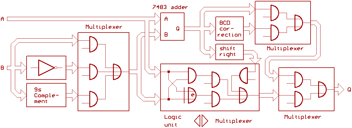
...But now back to the Wang 700.
Which went mentioned in ALU design, part 5.
The multiplexer at the left selects, if the adder B input is fed
by the 1s complement of B (for binary A-B),
by the 9s complement of B (for BCD A-B),
or by B (for binary/BCD A+B).
Actually, the multiplexer output is labeled TB
in the original schematic...
and I'm leaving out a few little details.
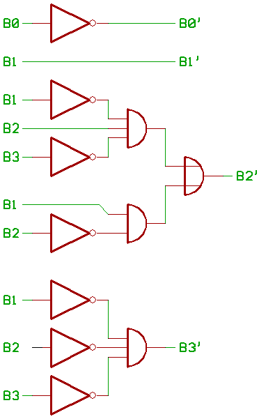
To make the set complete, I'm showing you the Wang 700
9s complementer again:
And now for the BCD correction.
(I'm simplifying quite a few things here).
The AND OR combination gates at the right side of the
schematic (connected to the blue marked control signals)
are a multiplexer, which either bypasses the BCD correction
(by feeding Z3..0 and C_OUT' from the adder outputs), or which
puts the BCD correction circuitry between the adder outputs
and Z3..0 / C_OUT'.
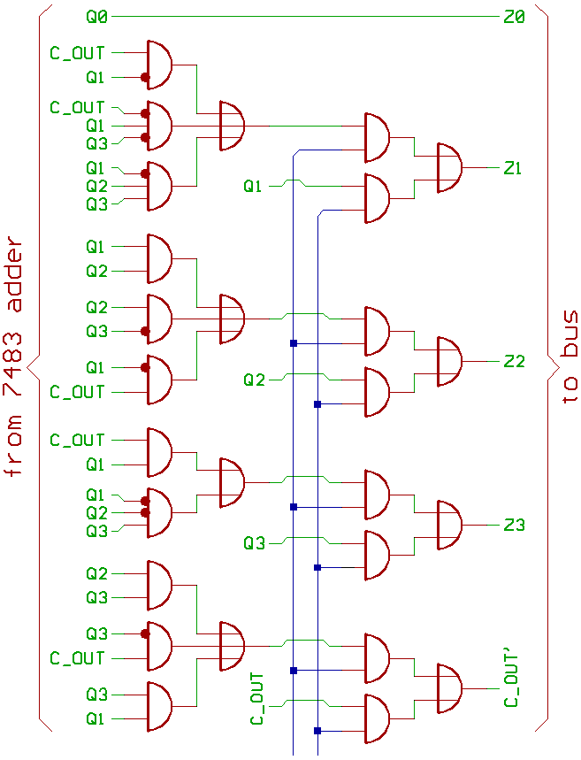
The basic idea behind this BCD correction circuitry is simple:
if the adder result isn't greater than 9
(and the adder output carry C_OUT = 0),
the result is a valid BCD number,
so it is passed through unchanged.
If the adder result is greater than 9
(or the adder output carry C_OUT is 1),
the result isn't a valid BCD number.
So the BCD correction circuitry sets C_OUT' to 1,
and adds +6 to the adder result.
For instance: if the adder output is decimal 11
(binary 1011, hexadecimal 0x0b), adding 6 will give us
decimal 17 (hexadecimal 0x11, binary 10001).
So if the adder result is decimal 11, the BCD correction
circuitry places decimal 1 on the Z3..0 outputs, and sets the C_OUT'
output carry to 1 (because the adder output was greater than 9).
That's all there is to it.
[HOME] [UP]/ [BACK] [1] [2] [3] [4] [5] [6] [7] [8] [NEXT]
(c) Dieter Mueller 2012