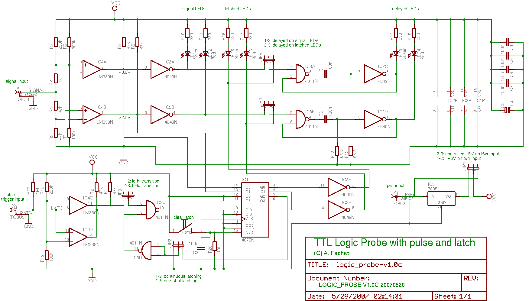
Logic Probe
This page describes a logic probe that can be used to analyze and debug TTL circuits.
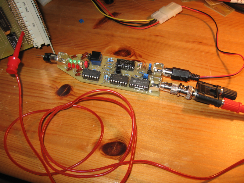
The logic probe is a small device with a sampling tip, and a number of LEDs that indicate the state of the signal connected to the sampling tip. Two "direct" LEDs show whether the signal is high (red LED), low (green LED), of unconnected (no LED). If the signal switches quickly between the two states, both LEDs seem to be on continuously (although they aren't).
A pulse logic detects transition to a state (HIGH or LOW) and generates a ca. 0.5sec pulse lighting up separate "pulse" LEDs. So a state change can be detected, even if it is only a short pulse invisible on the direct LEDs.
Additionally a second signal input can be used to latch the main signal at a low-high or low-high transition of the latch input.
Table of content
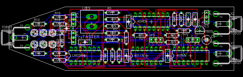
Version: 1.0C
Status: prototype
Notes
| This board has the connectors fixed, as well as the inversion of the latch LEDs. | |
| The layout is untested. | |
| The built in op-amp has a delay time of at least 300ns as far as I understand. So this probe is unfortunately not good enough for clocks, and only possibly working for address and select lines. |
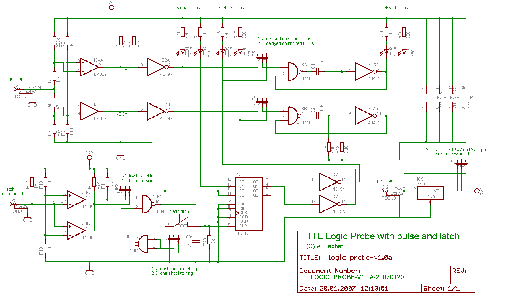
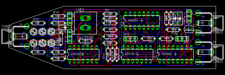
Version: 1.0A
Status: prototype with bugs
Notes
| Watch out, this board has the signal and latch input connectors exchanged, as well as the latch LEDs are inverted. | |
| I have yet to determine whether I have a problem with my selfbuilt computer, or the probe is not good enough for higher signal frequencies. Probably have to reduce the input resistor network values to reduce the RC constant. |
Files
| logic_probe-v1.0a.sch | |
| logic_probe-v1.0a-sch.png | |
| logic_probe-v1.0a.brd | |
| logic_probe-v1.0a-brd.png | |
| logic_probe_v1.0a.png(signal tip, pwr and latch input are connected via Cinch plugs.) |