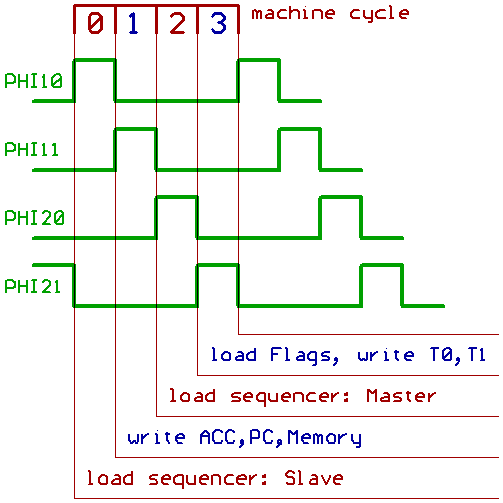
MT15 uses a 4_phase (non_overlapping) clock.
It appeared to be the most reliable approach for driving
master/slave_flipflops, built from transparent latches.
Instruction sequencer uses a three Bit counter,
build with master/slave_flipflops.
First step (PHI10) is, to update those slave_flipflops,
advancing the instruction sequencer to the next step.
The decoder logic is build with fast CTL gates, so the
control signals are supposed to be stable for the next step.
Next step (PHI11) is, to write ACC, PC, or memory.
Also, the carry master flipflop is updated
(we are discussing that part later).
Then (PHI20), the ALU performs an operation between
a register (ACC, PC) and memory, while the master
flipflops of the instruction sequencer are loaded
for preparing the next machine cycle.
Finally (PHI21), temporary registers (T0, T1) and flags
will be written.
OpCode may also be transferred into the Instruction Register
during PHI21 is active.
Clock generation with TTL logic, using 74164/7427:
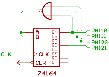
Did use a 74245 for buffering the 74164 outputs.
74164 input clock is 2MHz, so MT15 runs with 500 kHz.
So much for the clock signals.
[HOME] [UP]/ [BACK] [1] [2] [3] [4] [5] [6] [7] [8] [NEXT]
(c) Dieter Mueller 2005