

 |
Vic 20 ISA slot timing by Lee Davison. |

|
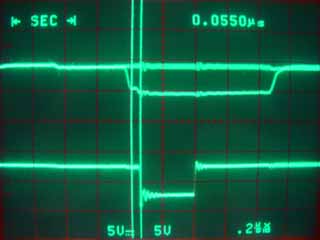
With all the wires going to the right places the 3Com card wasn't talking. After a go with the logic analyser revealed that the correct bytes in the correct order were being sent to the card a closer look at the access timings seemed to be called for. A short bit of test code that writes repeatedly, and regularly, to the I/O block used produced the following display.
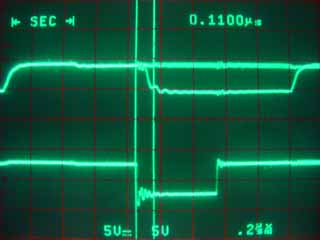
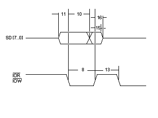
The fixLooking at the spec for ISA 8 bit I/O cycles gives a minumum figure for 11 (write data setup) of 7 to -45ns, that is 7ns before to 45ns after IOW goes low. A quick check on the scope reveals that on the interface the data is not stable for at least 110ns after IOW has gone low. Faliure because of this also shows that the I/O data is latched by the leading edge of the IOW signal and not by the trailing edge as I would have expected.
The easy way to fix the write problem would be to just delay the 6502 phase 2 signal, this is done using a 150ns hybrid delay line removed from an old DRAM memory card. Unfortunately this effects both the read and write timing and it would also mean the delayed phase 2 is active after the processor has finished it's cycle.
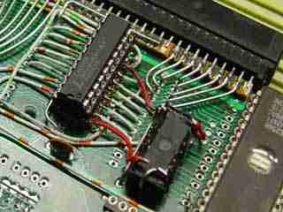
The solution is to only delay the leading edge of phase two, by combining the delayed phase 2 with the original phase 2, and to only do this on the write cycle. This almost worked but it turns out that the address lines also need to be stable before IOW or IOR go active so both read and write cycles were altered.
Fortunately there was one unused pin on the GAL so it was just a case of feeding the delayed phase 2 to this pin and adding the delayed phase 2 to the equations.
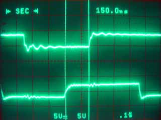
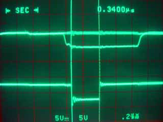
This done the test code was run again giving the trace shown below. The data is now stable before IOW or IOR goes low. The side effect of this is to reduce the active width of all I/O cycles. The timing spec says that this should be 541ns for an 8 bit I/O cycle but, as the card being used can also do 16 bit I/O transfers and the timing for them only requires a 165ns cycle, the 340ns as shown proved to be adequate.
With all that sorted perhaps now I can get my Vic 20 to work on my home network.
| Last page update: 1st March, 2004. | e-mail me
 |