
 -------------------------------------------------------
| ...And god asked the stones:                          |
| "Do you want to become hardware designers ?"          |
| "No, we are not hard enough.",                        |
| the stones replied.                                   |
|                                                       |
| So god, in his infinite wisdom,                       |
| created something more stubborn than a piece of rock: |
| the German electronics nerd.                          |
|                                                       |
| But even the hardest stone may crumble...             |
 -------------------------------------------------------
TREX was an experimental 32 Bit TTL RISC CPU.
Back in 2006, I grouped up with a software guru...
and we did start this little project here...
unfortunately, the project is dead now, the guru is gone,
(I fully understand that, and we parted as friends),
...and the PC with all the software tools and most of
the project files had a hard disk crash.
And as usual, there were no backups.
First we had some thoughts about using transistors, but during
my DECL transistor logic experiments, two things went obvious:
First: Building reliable transistorised DECL gates turned
out to be
more difficult as I thought, same thing for distributing
the signals.
Second: It turned out to be hard to estimate the size of the CPU
(or the number of transistors).
Then I did stumble over some very cute 54LS181 ICs in a hobby shop,
and I could... not... resist.
Unfortunately, the control circuitry of the CPU never ran out of bugs,
and there was a day, when debugging it felt like visiting planet Klendathu.
And while debugging the CPU, I bumped into a burnout at my workplace
back in August 2008, what separated me from hobby electronics for a very
long time.
There is a random collection of some of the remaining (hardware related) files,
but please note that this stuff is unfinished, untested, and contains bugs.
Thou shalt not try rebuilding it.
Now the pictures:
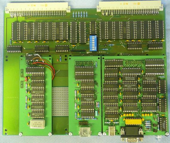
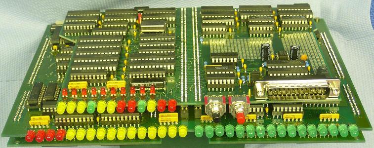
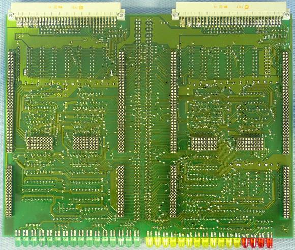
Peripheral/IO PCB.
Three modules can be plugged on top, and three modules at the bottom.
Currently, we have a timer, a PC keyboard interface, and a TTL UART.
The timer had some minor bugs, but they are fixed in the new PCB layout.
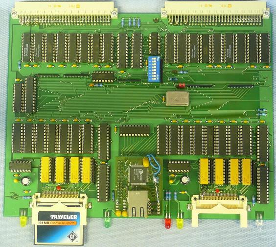
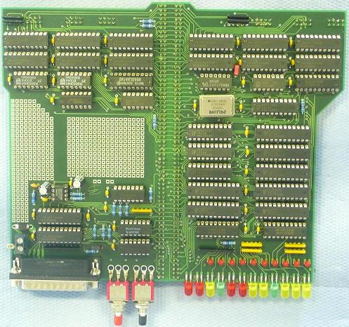
Ethernet and CompactFlash.
It would have been interesting to build a TTL based Ethernet controller,
but because it would have had only 10 MBit (and we already had enough other
important work to do), we decided against it.
Unfortunately, the DM9000 went out of production, and we had to modify
our design a little bit to go with the DM9010.
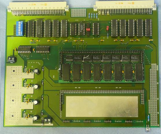
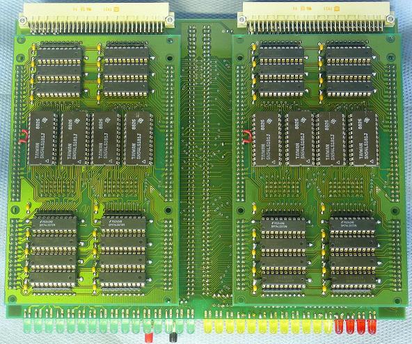
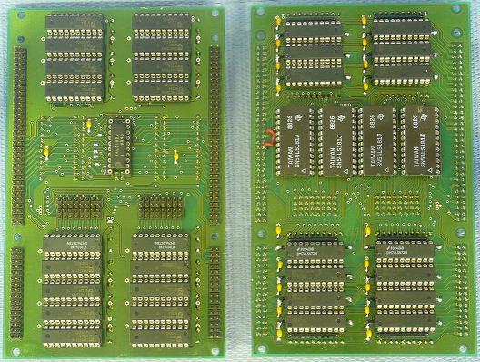
Memory PCB.
Note the little module plugged on top of the PCB.
It's a 4 layer PCB, with 8 SRAMS (512 kB each) on top, and 8 SRAMs at the
bottom. It's possible to plug up to 16 such modules into the big PCB,
which means two stacks (4 modules each) on top of the big PCB,
and 4 modules at the bottom.
Since one module carries 16 RAMs 512 kB each, the module has 8 MB RAM,
and the big PCB would be able to carry 128 MB of 15 ns SRAM in total.
Enough for running serious software...
Note: when defining one layer of a multilayer PCB as GND, make sure
that the PCB manufacturer _really_ knows about this,
else use GND polygons in the PCB layout.
The design also contains PCB space for four 3.3V regulators,
just in case that 5V SRAMs might go out of production.
Now for the CPU.
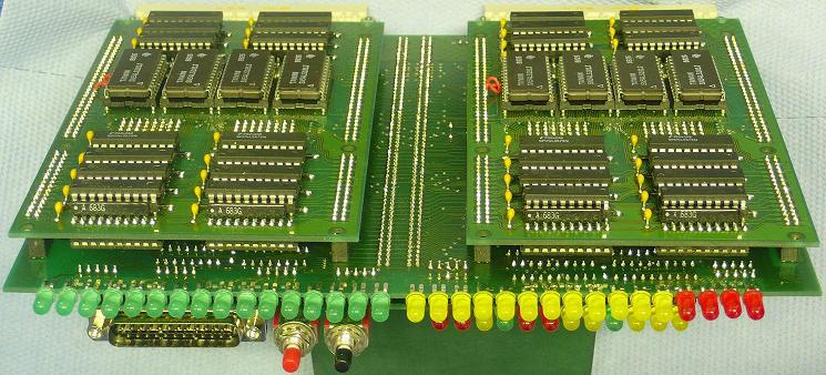
Some pictures from top, bottom, and the side.
The CPU is a neat, compact "sandwich".
The big PCB in the middle of said "sandwich" contains the bus interface
and the status register.
A closer view of the big PCB, note the "high density" connectors.
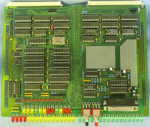
Three smaller PCBs are plugged into this big PCB:
The control PCB with the instruction latch/decoder/sequencer has 4 layers,
and contains quite a few GALs.
The other two PCBs carry 7 registers (biport register file built with 74574),
a shifter, and a 74181 based ALU.
Since each of the two identical PCBs/modules carries ALU and registers
for only 16 Bit, two modules are required for a 32 Bit CPU.
Note the ICs on top and at the bottom of the PCB.
Yep, 37 ICs in total (four of them DIP24) on a two layer PCB. :-)
The hard_to_buy 74182 can be replaced by a GAL if necessary.
The "TTAP port" of the CPU can be connected to the LPT port of a PC,
basically it's sort of a simplified JTAG interface, so it's possible to
start/stop/single_step a program, to execute an instruction sent by the
PC, and to read/write CPU registers...
which makes it possible to read/write CPU memory.
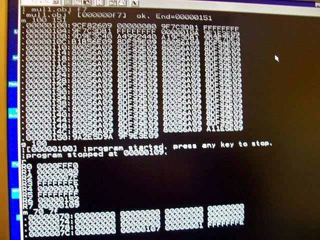
Here a screenshot of a test program, doing an unsigned 32 * 32 Bit
multiplication with a 64 Bit result.
So 0xffffffff * 0xffffffff = 0xfffffffe00000001, and the program worked.
So much for watching the remains of dead/extinct fossiles.
Rest in peace, my cute little dinosaur...
Looking at those pictures on a page in the internet is one thing.
But entering your workshop after a full year of absence, cleaning
up the desk from all those dead dinosaur guts is something
completely different.
Because when you take all those PCBs in your hands again,
you suddenly remember how much time and effort, how much
sweat and tears went into a project which seemed to be
doomed from the start...
And the thought that you wasted years of your life on
something like this can take it out of you.
More technical details in the "articles" section:
(c) Dieter Mueller 2008