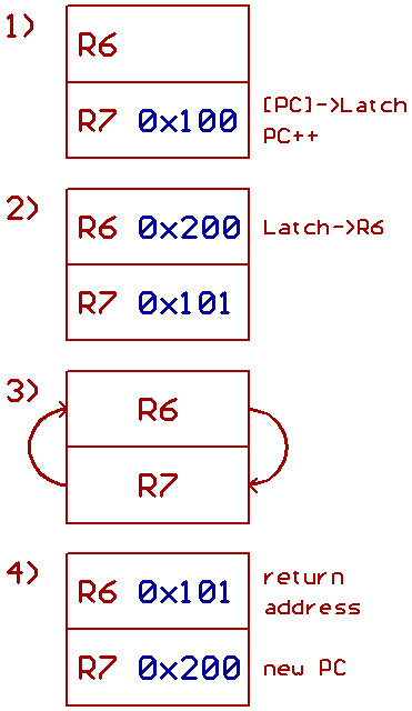
Now a short, simplified description about what happens when loading
a literal value into PC/R7, when Bit 31 of the instruction word is zero:
First, the contents of PC/R7 are placed on the address bus, and PC/R7
is incremented to point to the next instruction word.
The 32 Bit value from the data bus is sampled into a 74573 based latch.
Second, in the next cycle the value from the latch is loaded into LR/R6,
which worked as a temporary storage.
Third, PC/R7 and LR/R6 are swapped.
Fourth, the next instruction word is fetched from the new PC/R7 address,
while LR/R6 contains the "return address" of the instruction word which
follows the JMP/JSR instruction. It's easy.
"Oh my god, it takes three cycles and maybe an additional temporary register
when swapping the contents of PC/R7 and LR/R6 with that architecture !"
some of you might say.
In fact, I'm not swapping the contents of those registers, but the registers
themselves. The trick is to re_assign the control signals for both registers,
what basically takes four 2:1 multiplexers (74157), one D_Flipflop (7474),
and one XOR gate (7486)...
if I wouldn't have taken some GALs for building the control circuitry.
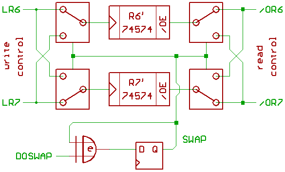
LR6, LR7 are control signals for loading R6, R7.
/OR6, /OR7 is the low_active output enable for both registers.
If SWAP is 0, R7' is R7/PC and R6' is R6/LR.
If SWAP is 1, R7' is R6/LR and R6' is R7/PC.
We are just throwing the switches, that's all.
If DOSWAP is 1, the flipflop which generates SWAP toggles with the start
of the next machine cycle, so swapping both registers takes no time at all.
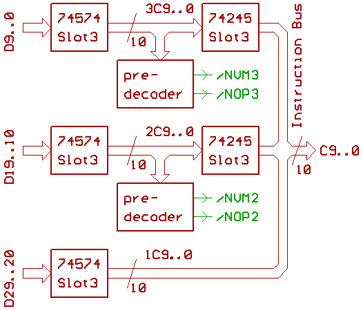
The instruction register is directly fed by the external databus, so fetching
a 32 Bit instruction word while incrementing PC takes one machine cycle.
If Bit 31 of the instruction word is zero, the word is directly loaded into PC
in the next cycle, and the interrupts will be disabled when fetching the next
instruction word, to make sure that there is a chance to save the return address
on stack when calling a subroutine.
If Bit 31 is 1, Bit 30 is used to enable/disable the interrupts when fetching
the next 32 Bit instruction word.
Bit 29..0 break into three 10 Bit instructions (or instruction triples).
Basically, there are three latches 10 Bit with output enable, which connect
to a 10 Bit CPU internal "instruction bus" which feeds the instruction decoder.
(there also is a 10 Bit shift register for "forging" an instruction from the
debugging interface into the instruction stream.)
We call each of the 10 Bit instructions a Slot. Slots are executed left to right,
starting with Slot 1 (Bit 29..20).
Slot 2 and Slot 3 have a predecoder, but from the timing diagram,
adding a predecoder to Slot 1 didn't make sense.
A predecoder has the purpose to strip some info from an instruction before it
enters the instruction decoder itself, the idea is to extract info if an instruction
might use the CPU external bus, or cause a change in program flow.
In our case, we use NAND gates to identify a MVM (move from/to memory)
which will cause a bus access to support bus arbitration, and a 74688 to
identify a NOP.
A NOP is defined as a register/register move which doesn't modify flags.
Detecting a NOP in Slot 2:
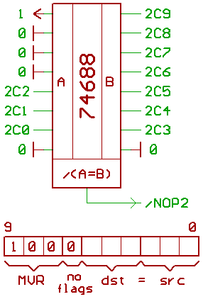
Detecting a MVM in SLOT 2:
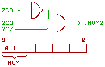
...same thing for Slot 3 with /NOP3 and /MVM3.
While analyzing code, it appeared that when using assembler macros, there is
a high chance that Slot 3 (and sometimes Slot 2) may contain a NOP, so if the
CPU detects a NOP in Slot 2 or Slot 3, that slot is skipped.
(If you want to have a NOP which won't be skipped, maybe for programming
short time delays, use an OR instruction like R1|=R1 with "flag modify"
turned off.)
Since there is no predecoder for Slot 1, the CPU assumes that the bus is used
during instruction fetch and in Slot 1, so if you have a system with more than one
TREX CPU, try to optimize the code in a way that a memory access happens
in Slot 1 to make bus arbitration a little bit more efficient.
One final word about the instruction decoder:
we have two 7410 NAND gates.
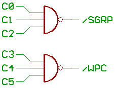
The /SGRP signal indicates, that the instruction might be a single operand
instruction (please take a look into the "TREX instruction set" article for
more details).
/WPC indicates, that the destination register is PC.
So a MVM, MVR, ADD (INC/DEC) with this signal active will trigger
the PC/LR swap mechanism.
[HOME] [UP]/ [BACK] [1] [2] [3] [4] [5] [6] [7] [8] [NEXT]
(c) Dieter Mueller 2007, 2008