
First, the inevitable foreword:
For every CPU, there is supposed to be a predetermined procedure,
what to do, and in what kind of order things should happen inside.
Like, what to do with ALU (arithmetic logic unit), registers, AddressBus
and DataBus interface, etc.
My first CPU, M02, binary compatible to the 6502, had 256kB
of microcode ROM (actually four 27512 EPROMs, 64kB each).
Decoding/executing a CISC_like instruction set can be tough,
and microcode (as some kind of program, hidden inside the CPU)
could ensure a high flexibility.
Means, it could be modified/changed with a (more or less)
reasonable amount of time and effort.
Problem is, that it may take a lot of ROM.
Sure, there are some tricks, how to reduce ROM size.
If things go wrong, you may end up with a computer inside
the computer, what puts a limit to the maximum speed of the CPU.
For more details, please consult/dissect the AM2910 datasheet.
Another source of information might be my article about
microprogramming.
My second CPU, the one_Bit M14500, was built for increasing
knowledge and testing concepts.
A one Bit CPU, with 16 instructions, and one addressing mode,
happens to be a nice playground for testing RISC like concepts
with a minimum of cost and effort.
Instruction decoding/sequencing could be done with only a few logic gates.
Of course, the practical use of such a design is, somewhat, limited.
MT15 is a mostly transistorised CPU.
For some reason, the use of microcode by building transistorised
"EPROMs" appeared to be a bad idea.
Wiring logic gates together would probably have been a solution.
Problem is, that some of the gates would have a lot of inputs,
and some would have not... resulting in a strange/chaotic contraption,
that would be (nearly) impossible to modify/change.
Experience showed, that such a design would require more than one try
(or modification), to work as intended.
But there is another solution: PLA, programmable logic array.
We now skip modern devices (like GAL22V10), ignore some of the
older things (as PAL16L8), way back before the stone age (74S330),
on our journey back towards the very basics.
Now introducing: a transistorised "programmable" logic array,
also known as PLA.
"Programmable" with a solder iron.
Well.
One PLA module has 18 input lines (started experimenting with 16,
but needed two more).
We have 16 AND gates, max. 18 inputs each, connecting to said
input lines. Followed by 10 OR gates (feeding the 10 output lines),
that may connect to the outputs of our AND gates.
Note the 16 vertical lines inside the schematic above.
Each one of those lines (also known as "the axis of evil"), may be
build with up to 18 PNP transistors (BC857), working as AND gate,
and up to 10 NPN transistors (BC847), working as OR gates.
Basically, it is build with CTL, complementary transistor logic.
We could have used diodes instead.
But point is, that transistors are nowadays (this article was written
in 2005) in the same price range, while being faster, with a remarkable
DC current gain.
That allows us to build rather large and "fast" logic arrays.
Downside is, that transistors have three pins.
Note: each one of the 10 output lines must be terminated with a
330 ohm pulldown resistor.
Those resistors are located on the mainboard (that carries five such
PLA modules).
Trick is, that outputs of (for instance) two modules could be wired
together to one pulldown resistor, turning two 10_input OR gates into
one 20_input OR gate, distributed/located in two different PLA modules...
that may have different input signals at the AND input lines.
Now a very simplified diagram, how the logic block (build with 5 PLAs)
is connected:
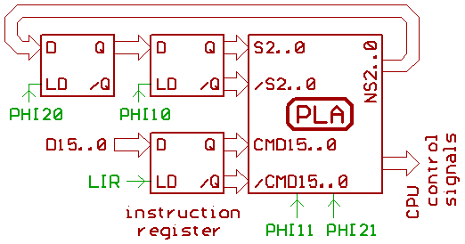
We happen to have a three Bit state machine, with S0..2
as the current state and NS0..2 as the next/following state.
Note the master/slave_flipflops, loaded with two non_overlapping
clock signals:
PHI20, PHI10.
Three Bits in a master/slave configuration means six flipflops.
Note, that the outputs (inverted and non_inverted) of the slave
flipflop are connected to PLA inputs, because our PLA modules
don't have integrated inverters, like PALs/GALs.
Additionally, we also have the 16 Bit OpCode, loaded at the
beginning
of the instruction execution with LIR into
the instruction register.
This also may be a source of information to the PLA, what to do,
and what step to take next.
Like performing calculations for a given addressing mode,
for instance.
Some PLA outputs, that control load/clock_signals for some
other registers/flipflops
(like the LIR signal), are gated
inside the PLA by two clock signals:
PHI11 and PHI21.
To be on the safe side, I decided to buffer those PLA outputs
with four 74HCT245 (the only TTL ICs inside MT15).
I know, that clock gating is evil, but it doesn't take
much transistors.
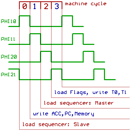
To clarify things, we take a short look at the clock signals,
already mentioned in my previous article:
The MT15 architecture.
[HOME] [UP]/ [BACK] [1] [2] [3] [4] [5] [6] [7] [8] [NEXT]
(c) Dieter Mueller 2005