 --------------------
| Improve the world, |
| kick a spammer.    |
 --------------------
2013: After nearly 5 years of absence from hobby electronics,
I built a 6502 single board computer for getting started again.
So please don't complain if things look less clean
than in my old/previous projects.
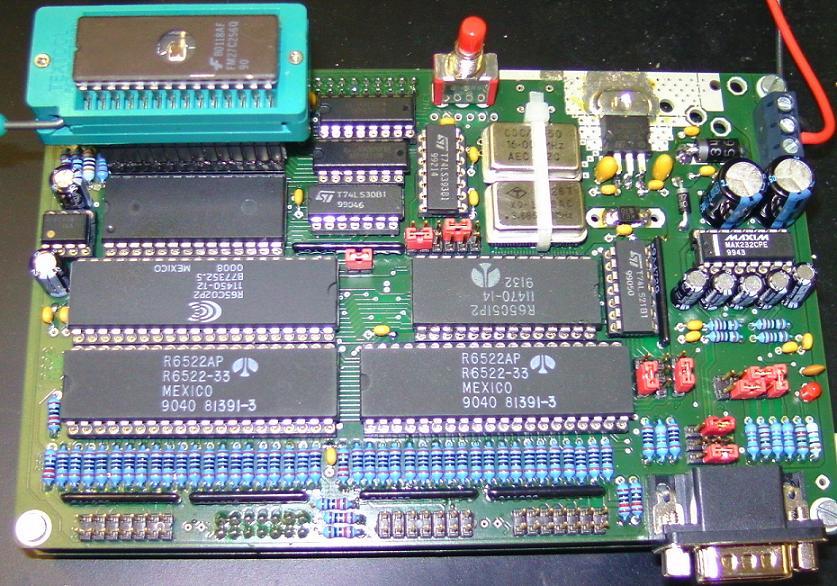
DRC2 is (more or less) based on Daryl Rictor's SBC2.
// I just like the elegance/simplicity of the SBC2 concept.
CPU: Pin 1 of the 6502 can be connected to GND with a jumper,
so it's possible to use a WDC 6502 and non_WDC 6502.
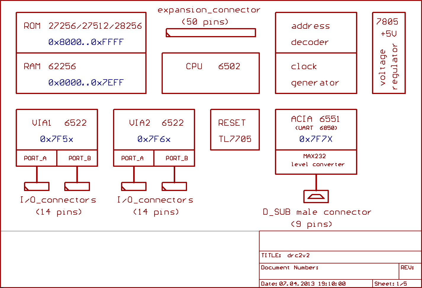
Memory map: I'm using the same address decoder as the SBC2.
$0000..$7EFF RAM
$7F50..$7F5F first 6522
$7F60..$7F6F second 6522
$7F70..$7F7F 6551 (alternatively 6850)
$8000..$FFFF ROM
RAM: 32 kB RAM... minus the I/O space.
ROM: always 32 kB.
27256 EPROM, 28256 FLASH...
or a 27512 EPROM with the upper or lower half of it's 64 kB
mapped to CPU memory, depending on the jumper setting.
I/O: 2 * 6522, 1* 6551.
9 pin male SUB_D connector for RS232.
The pinout for I/O connectors and bus expansion connectors
is supposed to be compatible to the SBC2.
To be on the safe side, I inserted 100 Ohm resistors
between the 6522 I/O pins and the I/O connectors.
Interrupt signals from the 6522s and the 6551 are ANDed
together by using a 7421, so it's possible to use ICs from WDC
(which have a push/pull output) and ICs from other vendors
(which have open collector output).
Reset: TL7705.
It isn't the best reset IC out there, because it is sensitive
to spikes in the power supply, and it probably won't work well
if VCC is below 3.6V...
but I had some of those ICs in the drawer.
Clock: Two TTL metal can oscillators, plus a 74393
and some jumpers for dividing down the oscillator outputs:
16 MHz oscillator -> 4, 2, 1 MHz for the CPU,
3.6864 MHz oscillator -> 1.8432 MHz for the 6551 ACIA.
// Decided against building oscillators by using 7404 TTL gates
// for reliability reasons.
After building the first prototype, I had to notice that it's
a bit difficult to buy the 6551 ACIA, so I added the feature
of alternatively using a 6850 UART as an afterthought\kludge.
Unfortunately, there only was place at the bottom of the PCB
for integrating the IC socket for the 6850, and when using a 6850,
the 3.6864 MHz oscillator has to be replaced by a 2.4576 MHz oscillator,
because there wasn't enough PCB space for implementing a :3 divider,
sorry.
// Note to myself: next time, better leave enough space in your
// PCB layout for soldering in a ZIF (zero insert force) socket later.
// This simplifies testing/debugging software.
During the test runs, I noticed that "overclocking" the SBC at 4 MHz
(not with the ICs shown in this picture, of course)
is possible with some 65Cxx parts, but I wouldn't recommend this
for reliable operation of the SBC.
For interfacing a PS/2 keyboard to a 6522, I'm using this here:
Basically two 74164 shift registers for serial/parallel conversion,
and a 74HC14 based retriggerable monoflop which recognizes the end
of the data transmission from the keyboard and latches the data
from the shift registers into a 74574.
...had no 74595 in the drawer, sorry.
Wanted to have a simple interface without using a microcontroller.
Downside is, that it isn't possible to write data to the PS/2
keyboard for changing repeat rate, turning on/off the LEDs etc.
I plugged the module to port A of the 6522 at 0x7F5x,
a rising edge on CA1 indicates that a valid Byte
which was sent from the keyboard is at PA7..0.
Now to present the D04 CRT/LCD controller to the public.
Please be aware, that D04 is sort of a "crude hack"...
because compared to D03 (which offered a similar functionality),
D04 has about half the size of D03.
If I would build somehing like this again,
I sure would do a few things quite different... :)
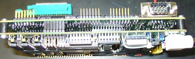
DRC2 (single board computer) and D04 (CRT/LCD controller)
are mounted together as a "sandwich":
D04 can display monochrome 40*25 text,
and 320*200 graphics (similar to the C64 HIRES format).
It also can display both things simultaneously,
mixed together by 7486 XOR gates.
// note: 7486 (XOR gates) and 7432 (OR gates) have identical pinout.
D04, the CRT/LCD controller PCB:
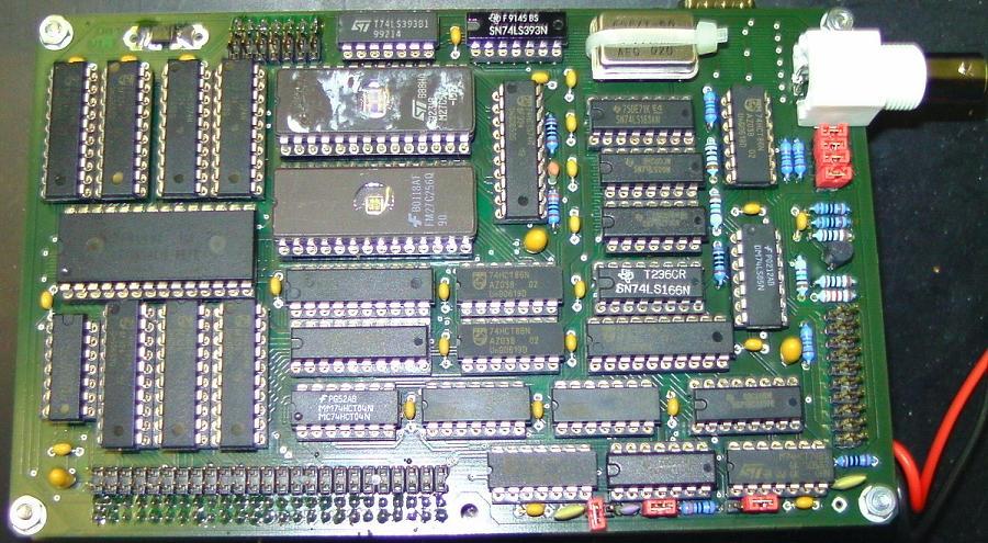
It can drive a CRT and a 320*240 LCD in parallel
(at least in theory). 50 Hz vertical sync.
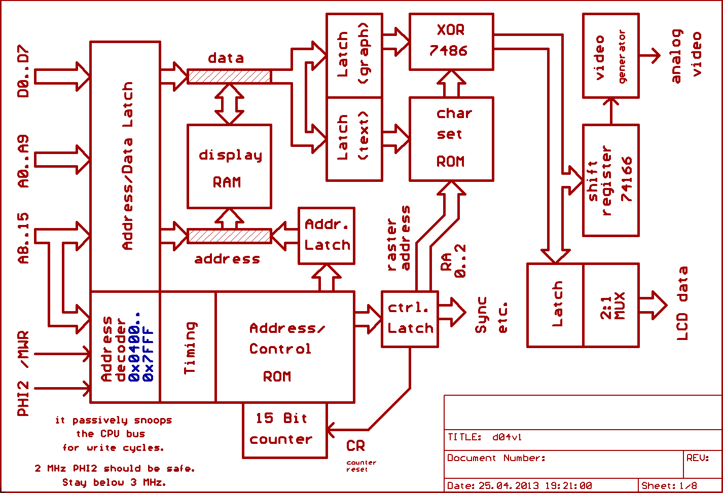
D04 "snoops" the 6502 bus for write cycles to 0x0400..0x7fff,
holds address and data in 74574 latches, and performs one write
cycle per microsecond into its own display memory.
So the CPU RAM is "mirrored" into the CRT RAM.
The advantage of this approach is, that D04 runs independent
from the CPU with its own clock generator.
During the test runs, it worked with CPU speeds up to 4 MHz,
but I would not recommend to go beyound 2 MHz to be on the safe side.
// For instance, STA ABS has 3 read cycles, one write cycle.
For generating display memory adress and sync/control signals,
I'm using a 15 Bit counter (2 * 74393), plus a 27512 EPROM
which contains a lookup table.
I'm using port B of the 6522 at 0x7F5x to configurate the
CRT/LCD controller: selecting which 1 kB text page is displayed,
turning on/off graphics, selecting an 8 kB graphics page, etc.
There wasn't enough PCB space left to integrate a 74273 etc.
into D04 for doing this, sorry.
PB4..PB0: selects the text     page to be displayed (32 pages, 1 kB each)
PB6..PB5: selects the graphics page to be displayed ( 4 pages, 8 kB each)
PB7     : = 0 enables graphics (default: 1)
CB1     : senses the 50 Hz vertical sync of the CRT/LCD controller
CB2     : switches the character set to be displayed (default: 1)
There sure is a lot of stuff on that PCB,
because running the timing independent from the CPU,
supporting a LCD and displaying text plus graphics
bloats the design a little bit.
// If you would be displaying only text, coupled to the CPU timing,
// without graphics and LCD, the design sure would be a lot smaller.
Some further experiments:
(hand wired stuff without layout and schematic)
Implemented something like a SPI interface by using
a 6522 shift register plus a 74164 for receiving the Bits.
Wrote sort a basic driver for initializing a MMC card,
looks like reading a 512 Byte block from the MMC worked.
Didn't try to _write_ the MBR, sorry.
BTW: since the MMC runs at 3.3V, I'm using a 74LVC245
as a level converter for the SPI interface.
Also, I tried connecting the ENC28J60 Ethernet controller IC.
But the problem with the 6522 is, that the clock output for the
shift register is high by default.
From the datasheet, the ENC28J60 insists to have SCK low
for at least 210 ns before chip select goes inactive...
else, it isn't possible to read/write the MII/PHY registers
of the ENC28J60.
Fixed the problem with a 7474 flipflop, which is set
at the first rising edge of the 6522 shift register clock output,
and reset by another I/O pin of the 6522 before chip select
is turned inactive.
The clock output of the 6522 is ANDed by using a 7408 with
the output of that flipflop to generate a propper SCK signal
for the ENC28J60.
Initializing the ENC28J60 worked, and I was able to copy
multicast packets from the controller to CPU memory when
connecting said controller to a PC by using a CAT5 patch cable.
Woot.
But my problem now is, that I'm not much of a coder. :)
As for April 2013, I don't dare to place code which looks
that ugly into public, sorry.
This all was enough work for now, and I'm now taking
a break before trying to figure out what to do next.
Download and rebuild this at your own risk.
I'm intentionally trying to keep things a bit messy and chaotic:
First, because this saves me time.
Second, because this reduces the interest/value for commercial use.
(c) Dieter Mueller 2013