|
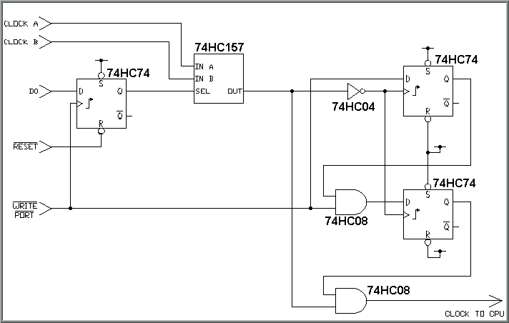
Clock A and Clock B are the two separate clock inputs
D0 is the processor D) data line
Reset is the processor reset signal
Write Port is created by gating together the address select signal, R/W and phase2. It should pulse low while phase 2 is high and the CPU is writing to the clock speed select circuit.
How the circuit works
When the CPU changes the clock speed, the Write Port line goes low. At the end of the write cycle, the currently selected clock goes low, which loads the low Write Port signal into the two right-hand flip-flops. The lower flip-flop then holds the clock output to the CPU low via the lower of the 2 and gates.
After a delay of a few nanoseconds, determined by the propagation delay in the logic that creates the Write Port line, the Write Port line will go high, loading the left-hand flip-flop with the clock select signal. This then selects the desired clock signal via the 74HC157 multiplexer.
The clock pulses clock a high state into first the upper and then the lower of the two right-hand flip-flops. Until the second flip-flop goes high, the CPU clock line is held low. This generates a delay of between one and two cycles of the new clock, during which the CPU clock is held low.
Since the output of the flip-flop which gates the CPU clock changes when the clock line is already low, there are no switching glitches fed through to the CPU clock.
Expanding to more than than 2 clock speeds
If desired, the left-hand flip-flop could be replaced with a latch such as the 74HC175, 74HC174 or 74HC273, latching 4, 6 or 8 bits of data from the processor. The 74HC157 could then be replaced with a larger multiplexor to select between more clock inputs. The latch IC used should be a type with a reset input, so the system boot-up speed can be set to the apropriate clock source.
Note : A 2-cycle CPU delay will be generated whenever the port is writen to, whether the clock speed is changed or not. For this reason, it is inadvisable to use any spare bits of the speed-select port to control something else.
|
|

